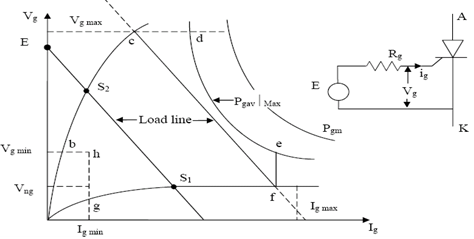
The gate circuit of a thyristor behaves like a poor quality diode with high on state voltage drop and low reverse break down voltage. This characteristic usually is not unique even within the same family of devices and shows considerable variation from device to device. Therefore, manufacturer’s data sheet provides the upper and lower limit of this characteristics as shown in figure below. Each thyristor has maximum gate voltage limit (Vgmax), gate current limit (Igmax) and maximum average gate power dissipation limit (PGav/Max). These limits should not be exceeded in order to avoid permanent damage to the gate cathode junction. There are also minimum limits of Vg (Vgmin) and Ig (Igmin) for reliable turn on of the thyristor. A gate non triggering voltage (Vng) is also specified by the manufacturers of Thyristors. All spurious noise signals should be less than this voltage Vng in order to prevent unwanted turn on of the thyristor.
Referring to the gate drive circuit in the inset the equation of the load line is given by
Vg = E – Rgig
Gate Drive Requirements
- Positive gate voltage or gate current
- Maximum Permissible gate power dissipation PGM
- There are maximum and minimum limits for gate voltage and gate current to prevent the permanent destruction of junction J3 and to provide the realizable triggering.
- The gate signal can be ac or dc or a sequence of high frequency pulses.