Sample & Hold Circuit is used to sample the given input signal and to hold the sampled value. Sample and hold circuit is used to sample an analog signal for a short interval of time in the range of 1 to 10µS and to hold on its last sampled value until the input signal is sampled again. The holding period may be from a few milliseconds to several seconds.
The following figure shows the block diagram of a typical sample and hold amplifier.
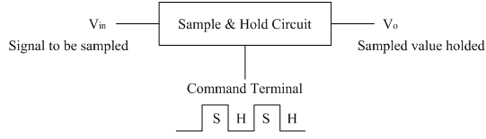
The Command terminal is in the form of a logic pulse. It controls whether to sample the input signal or hold the last sampled value of the input signal. When the pulse is high signal is sampled and when the pulse is low signal value is holded. Thus the circuit has two modes of operation depending upon the logic level of S/H command signal.
Upon receiving the input command pulse, the circuit samples the input and output follows input i.e. output tracks the input so called TRACK mode of operation. After command pulse is removed the circuit holds the output at a value which input signal had at an instant of pulse deactivation; which is called HOLD mode.
Sample and hold circuits are used in following applications.
1. Analog to Digital conversion (ADCs)
Out of different ADCs, successive approximation type ADC uses S/H circuit, where the signal is to be held constant while A to D conversion is taking place.
2. In DACs
3. In analog demultiplexing in data distribution and in analog delay lines.
In general S/H circuits are used in all applications where it is necessary to freeze the analog signal for further processing.
The following figure shows a typical sample and hold circuit using op-amp.
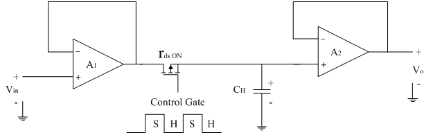
Amplifier A1 and A2 are both voltage follower circuits. FET is operated as ON/OFF switch. The S/H pulses controls the switching ON/OFF of FET.
Signal to be sampled is applied at Vin. Input impedance of A1 is very high so input voltage source is not loaded. While sampling output of A1 is same as Vin.
When S/H pulse is applied FET switches ON and starts conducting. Resistance between drain and source (rdsON) is very small.
For voltage follower, A1 and A2 have 100% feedback (β=1). Therefore output impedance of A1 and A2 is very small. Now capacitor C starts charging through rdsON and output impedance of A1.
Charging Time Constant = rdsON × rout × C
As rdsON and rout are very small, capacitor C charges through very quickly to Vin (i.e. capacitor tracks the input signal). At the end FET is off, so almost acts as open circuit. So capacitor isolates from previous circuits and it holds the charge of last sampled value.
As input impedance of A2 is very large, capacitor discharging time is very high, so it almost holds the charge. Also Gain of A2 is unity.
Therefore
Vout = Charge on capacitor
As rout of A2 is very small, we can take Vout across any value of RL
The Capacitor C used has a perfect dielectric having no leakage. Materials used for di-electric are polycarbonate, polythene, polystyrene, myler or Teflon.
Performance parameters of S/H circuit:
The performance of an ordinary S/H circuit can be characterized by Vio, Gain error, nonlinearity etc. Consider the following figure to define some of the important parameters of S/H amplifier.
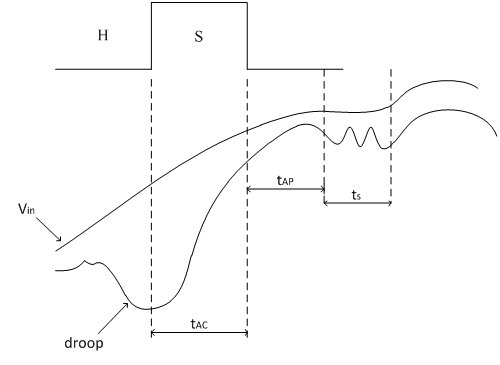
1. Acquisition Time (tAC):
It is the time required for the holding capacitor CH to charge upto a level close to the input voltage during sampling. It depends on three factors namely RC time constant, Maximum output current of op-amp and slew rate of op-amp.
2. Aperture Time (tAP):
Ideally as soon as the hold command is given to S/H circuit, the circuit should stop following any changes taking place in the input and hold the latest sampled value. But practically, the S/H circuit will follow the changes in input voltage for a short period of time, even after receiving the hold command. This period is called as aperture time. It is due to the propagation delays of the driver and the switch.
3. Aperture Uncertainty (∆tAP):
It is the variation in the aperture time from sample to sample.
4. Hold mode settling time (ts):
After the application of hold command, it takes a certain amount of time for Vo to settle within a specified error band such as 1%, 0.1%, 0.01%.
5. Hold Step:
At the time of switching from sample to hold or hold to sample mode, there is an unwanted transfer of charge between the switch driver and holding capacitor CH. This changes the capacitor voltage and hence output voltage. These changes in output voltage are referred as hold step, pedestal error or sample and hold offset.
6. Feed through:
In the hold mode, because of stray capacitances across switch there is a small amount of ac coupling between Vo and Vin. This ac coupling causes output voltage to vary with variation in the input voltage. This is referred as feed through.
7. Voltage Droop:
The leakage current causes voltage of the capacitor to drop down. This is referred as droop.
This sample and hold circuit is readily built in IC form is available (monolithic) and are comparatively inexpensive. For this IC user has to connect only a single capacitor externally. National Semiconductor ICs LM 198/298/398.