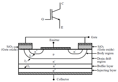
The major between insulated gate bipolar transistor and MOSFET is that, the corresponding MOSFET cell structure lies in the addition of a p+ injecting layer. This layer forms a pn junction with the drain layer and injects minority carriers into it. The n type drain layer itself may have two different doping levels. The lightly doped n- region is called the drain drift region. Doping level and width of this layer sets the forward blocking voltage of the device. However, it does not affect the on state voltage drop of the device due to conductivity modulation in connection with the power diode. This construction of the device is called “Punch Trough†(PT) design. The Non-Punch through (NPT) construction does not have this added n+ buffer layer. The PT construction does offer lower on state voltage drop compared to the NPT construction particularly for lower voltage rated devices. However, it does so at the cost of lower reverse break down voltage for the device, since the reverse break down voltage of the junction J1 is small. The rest of the construction of the device is very similar to that of a vertical MOSFET including the insulated gate structure and the shorted body (p type) – emitter (n+ type) structure.
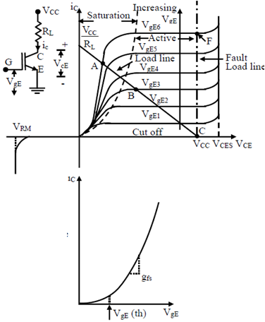
Steady state characteristics of an IGBT
The IGBT cell has a parasitic p-n-p-n thyristor structure. When the gate emitter voltage is below the threshold voltage only a very small leakage current flows though the device while the collector – emitter voltage almost equals the supply voltage. The device, under this condition is said to be operating in the cut off region. The maximum forward voltage the device can withstand in this mode is determined by the avalanche break down voltage of the body – drain p-n junction. As the gate emitter voltage increases beyond the threshold voltage the IGBT enters into the active region of operation. In this mode, the collector current Ic is determined by the transfer characteristics of the device. The ratio of ic to (VGE – vGE(th)) is called the forward transconductance (gfs) of the device and is an important parameter in the gate drive circuit design. As the gate emitter voltage is increased further Ic also increases and for a given load resistance (RL) VCE decreases. At one point VCE becomes less than VGE – VGE(th). Under this condition the driving MOSFET part of the IGBT enters into the ohmic region and drives the output p-n-p transistor to saturation. Under this condition the device is said to be in the saturation mode. In the saturation mode the voltage drop across the IGBT remains almost constant reducing only slightly with increasing VGE. In power electronic applications an IGBT is operated either in the cut off or in the saturation region of the output characteristics. Since VCE decreases with increasing VGE, its desirable to use the maximum permissible value of VGE in the ON state of the device.
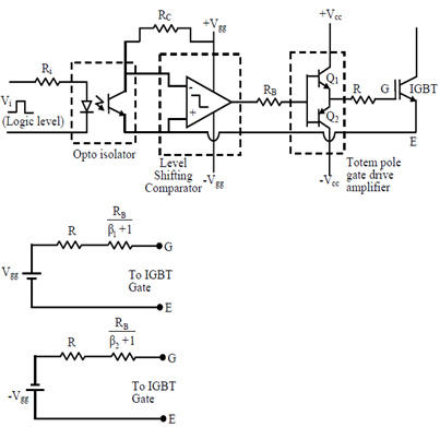
Gate Drive Circuitry of IGBT:
The gate drive circuit of an IGBT should ensure fast and reliable switching of the device. In particular, it should.
- Apply maximum permissible VgE during ON period.
- Apply a negative voltage during off period.
- Control dic/dt during turn ON and turn off to avoid excessive Electromagnetic interference (EMI).
- Control dVce/dt during switching to avoid IGBT latch up.
- Minimize switching loss.
-
Provide protection against short circuit fault.
The logic level gate drive signal is first opto-isolated and fed to a level shifting comparator. This stage converts the unipolar (usually positive) output voltage of the opto-isolator to a bipolar (±Vgg) signal compatible to the IGBT gate drive levels.The output of the comparator feeds a totem pole output amplifier stage which drives the IGBT. The equivalent circuit of the gate drive during turn on and off are shown in figure. If Vcc>Vgg then both Q1 and Q2 will operate in the active region and reasonably constant value of β1 & β2 of these two transistors can be used for analysis purpose.These equivalent circuits along with the model of the IGBT input MOSFET can be used to analyze the switching performance of the device. Conversely, for a desired switching performance a suitable gate drive circuit can be designed.