Home > Digital CMOS Design > Propagation Delay > RC Delay Model of NAND Gate
RC Delay Model of NAND Gate :
The propagation delay calculations for a CMOS gates is similar to that in static inverter.
During the delay analysis the transistor is modelled as a resistor whose value depend on the supply voltage and an equivalent resistance. The equivalent RC network contains the effect of internal node capacitances. Figure below shows equivalent RC switch level model.
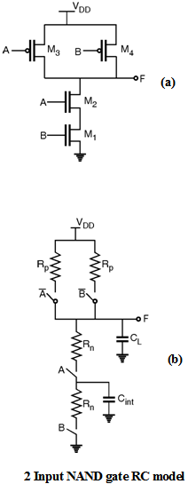
The propagation delay in complex gates depends upon the input pattern e.g. for low to high transition three possible input combinations can be identified for NAND gate that are (A = 0, B = 0), (A = 0, B = 1) and (A = 1, B = 0), which charges output to VDD. If both inputs are driven low (A = 0, B = 0) the two PMOS devices are ON. The delay in this case is 0.69 Rp2 CL since the two transistors are in parallel.
When only one PMOS device turns ON (i.e. either of A or B is low) the delay is called as worst case delay and is given by 0.69 Rp CL. For the pull down path the output is discharged only if both A and B switched to logic high (A = 1, B = 1) and the delay in this case is given as 0.69 (2 Rn) CL since the two transistors are in series. The important point here to note that we have ignored the effect of internal node capacitance Cint while calculating the delay.
Propagation Delay of 4 Input NAND Gate :
Consider a four input NAND gate as shown in Figure. The propagation delay calculated using Elmore delay model is given as,
tpHL = 0.69 [R C1 + (R1 + R2) C2 + (R1 + R2 + R3) C3 + (R1 + R2 + R3 + R4) CL]
For, RN = R1 = R2 = R3 = R4.
tpHL = 0.69 RN [C1 + 2 C2 + 3 C3+ 4 CL]