Home > Analog CMOS Design > MOSFET Amplifiers > Frequency Response of CS Amplifier
Frequency Response of CS Amplifier :
In our previous analysis of the CS amplifier we focused on low frequency characteristics neglecting the effect of device and load capacitances.
But, in many analog circuits there is trade-off between speed and many parameters such as gain, power dissipation and noise. Therefore it is necessary to understand the frequency response limitations.
An important phenomenon that occurs in many analog circuits is related to Miller effect which states that, when a circuit such as shown in Figure (a) is converted to equivalent circuit shown in Figure (b) then Z1 = and Z2 = where An = .
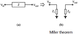
If 'I' is the current flowing through the 'Z' then the same current 'I' will flow thus 'Z1' as well as 'Z2'.
\ I = ; I = ; I =
\ =
i.e. Z1 =
Also, =
i.e. Z2 =
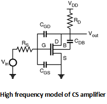
The high frequency model of the CS amplifier is as shown in Figure below.
The small signal model of the circuit can be drawn as shown in Figure below.
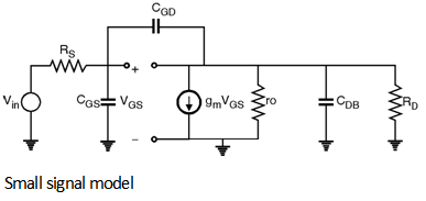
Using Miller effect for capacitor CGD.
We get, =
=
\ CGD1 = CGD [1 + gm (RD || ro)]
Similarly,
At output node, =
\ CGD2S = CGD
CGD
Thus the modified small signal equivalent circuit becomes as shown in Figure below.
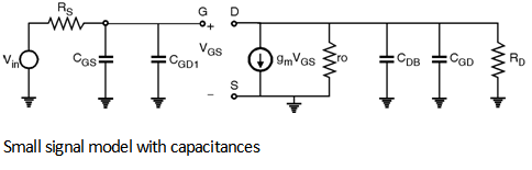
\ The pole associated at input node is :
Win =
also, the pole associated at output node is,
Wout =
\ The transfer function of the CS stage is given as :
=
The primary error in this estimation is that we have not considered the existence of zeros in the circuit. Another concern is the gain approximation of the amplifier by - gm
(RD || ro) whereas in reality the gain varies with frequency due to the capacitance at the output node.