Fault Modeling
Fault modeling is the technique to use stuck-at models the effects of the defects in an integrated circuit. This model is found to be more realistic when small-scale integration technology was established. However, the stuck-at model, for practical reasons, are still widely used in the EDA software tools. In this model an input or output of a logic gate is stuck to a logic value 0 or 1 and is not sensitive to signal event occurence from the signal that drives it. The models in digital circuits are created and the faults are injected into the model. The fault-free circuit and the faulted circuit are simulated and if the difference in response at an observable I/O pin then the fault is considered to be detected. The fault model is an image when compared to the various, complex kinds of defects that are occured in a system. Therefore, the predictions of test effectiveness based on the stuck-at model are having errors.
AND Gate Fault Model:
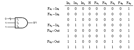
The AND gate shown in figure is fault-modeled for inputs and the outputs. This results in n + 2 tests for an n-input AND gate. The input tested is controlling input which determines the value appears on the output. Input pattern of all 1s tests for the output. It is not necessary to test for an output fault because any input test also detect the output. Further, output is detected without detecting any input fault if two or more inputs are at logic low.
OR Gate Fault Model:
An n-input OR gate, requires n + 2 tests. Further, the input values are the complement of the values for an AND gate. The input tested is set to 1 and all other inputs are set to 0.
Inverter Fault Model:
The Inverter is modeled with output. When failed to invert a transistor and both stuck-at faults are detected.