With the help of v-I characteristics we can easily explain the operation SCR, there are three modes of operation. v-I characteristics of SCR is a graph of anode current I A on y-axis & anode to cathode Voltage plotted on x-axis v-I characteristics can be split into two parts namely Forward Characteristics & Reverse Characteristics
Steady State Characteristics of SCR
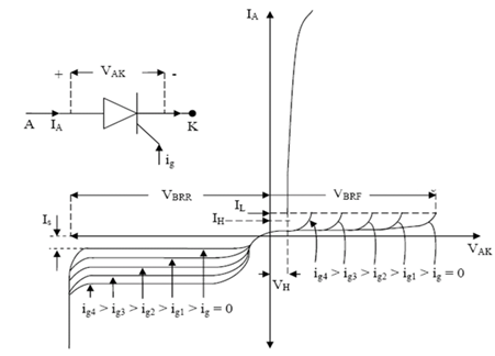
There are three modes of operation for an SCR depending upon the biasing given to it:
Forward blocking mode
In this mode of operation the anode is given a positive potential while the cathode is given a negative voltage keeping the gate at zero potential i.e. disconnected. In this case junction J1 and J3 are forward biased while J2 is reversed biased due to which only a small leakage current flows from the anode to the cathode until the applied voltage reaches its breakover value at which J2 undergoes avalanche breakdown and at this breakover voltage it starts conducting but below breakover voltage it offers very high resistance to the flow of current and is said to be in off state.
Forward conduction mode
SCR can be brought from blocking mode to conduction mode in two ways – either by increasing the voltage across anode to cathode beyond breakover voltage or by applying of positive pulse at gate. Once it starts conducting no more gate voltage is required to maintain it in on state. There is one way to turn it off i.e. Reduce the current flowing through it below a minimum value called holding current.
Reverse blocking mode
SCR are available with reverse blocking capability. Reverse blocking capability adds to the forward voltage drop because of the need to have a long, low doped P1 region. (If one cannot determine which region is P1, a labeled diagram of layers and junctions can help).
Usually, the reverse blocking voltage rating and forward blocking voltage rating are the same. The typical application for reverse blocking SCR is in current source inverters.
Switching Characteristics of SCR:
During Turn on and Turn off process a thyristor is subjected to different voltages across it and different currents through it. The time variations of the voltage across a thyristor and the current through it during Turn on and Turn off constitute the switching characteristics of a thyristor.
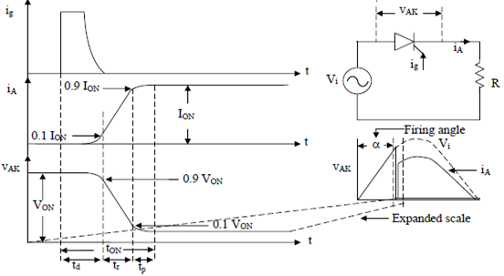
Turn on Switching Characteristics:
A forward biased thyristor is turned on by applying a positive gate voltage between the gate and cathode as shown in figure. Figure below shows the waveforms of the gate current (ig), anode current (iA) and anode cathode voltage (VAK) in an expanded time scale during Turn on. The total switching period being much smaller compared to the cycle time, iA and VAK before and after switching will appear flat. As shown in Figure there is a transition time “tON” from forward off state to forward on state. This transition time is called the thyristor turn of time and can be divided into three separate intervals namely, (i) delay time (td) (ii) rise time (tr) and (iii) spread time (tp).
• Delay time (td): After switching on the gate current the thyristor will start to conduct over the portion of the cathode which is closest to the gate. This conducting area starts spreading at a finite speed until the entire cathode region becomes conductive. Time taken by this process constitute the turn on delay time of a thyristor. It is measured from the instant of application of the gate current to the instant when the anode current rises to 10% of its final value (or VAK falls to 90% of its initial value). Typical value of “td” is a few micro seconds.
• Rise time (tr): For a resistive load, “rise time” is the time taken by the anode current to rise from 10% of its final value to 90% of its final value. At the same time the voltage VAK falls from 90% of its initial value to 10% of its initial value. Usual values of maximum allowable diA/dt are in the range of 20-200 A/μs.
• Spread time (tp): It is the time taken by the anode current to rise from 90% of its final value to 100%. During this time conduction spreads over the entire cross section of the cathode of the thyristor. The spreading interval depends on the area of the cathode and on the gate structure of the thyristor.
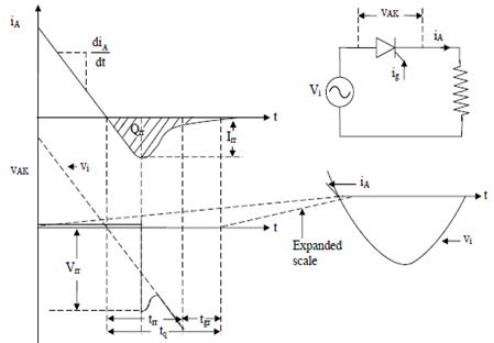
Turn off Switching Characteristics
Figure below shows the variation of anode current and anode cathode voltage with time during turn off operation on an expanded scale. Once the thyristor is on, and its anode current is above the latching current level the gate loses control. It can be turned off only by reducing the anode current below holding current. The turn off time tq of a thyristor is defined as the time between the instant anodes current becomes zero and the instant the thyristor regains forward blocking capability. During turn off time, excess minority carriers from all the four layers of the thyristor must be removed. Accordingly tq is divided in to two intervals, the reverse recovery time (trr) and the gate recovery time (tqr). The time interval tq = trr + tgr is called “device turn off time” of the thyristor. No forward voltage should appear across the device before the time t.