Home > Digital CMOS Design > CMOS Inverter
CMOS-Inverter
- Beta-Ratio-Effects
- CMOS-Inverter
- Dissipation-due-to-Direct-Path-Currents
- Dynamic-Power-Consumption
- Noise-Margin
- Power-Delay-Product-in-CMOS
- Power-Dissipation-minimization-Techniques
- Static-Power-Consumption
- VTC-CMOS Inverter
- Width-Length-Ratio-Calculation-of-CMOS
In this section we focus on the inverter gate. Table below shows the inverter truth table which shows that when there is '1' on the input, then at the output there is '0' and vice-versa.

Fig_CMOS-Inverter
Figure below shows the circuit diagram of CMOS inverter. The operation of CMOS inverter can be studied by using simple switch model of MOS transistor.
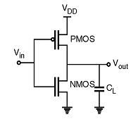
Fig CMOS-Inverter
When Vin is high and equal to VDD the NMOS transistor is ON and the PMOS is OFF(See Figure below). Hence direct current flows from Vout and the ground which shows that Vout = 0 V. On the other hand, when Vin is low then NMOS transistor is OFF and PMOS transistor is ON (See Figure below).
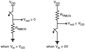
Fig2 CMOS-Inverter
Therefore, direct current flows from VDD to Vout and charges the load capacitor which shows that Vout = VDD. Therefore the circuit works as an inverter (See Table).
Properties of CMOS Inverter :
(1) Since in CMOS inverter there is existence of direct between power supply and ground, it has low output impedance.
(2) As the output voltage in CMOS inverter is always either VDD or GND, the voltage swing in CMOS inverter is VDD 0, hence VDD .
(3) As the gate of MOS transistor does not draws any DC input current the input resistance of CMOS inverter is extremely high.