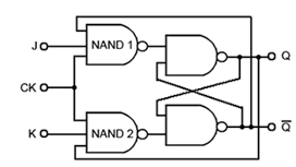
The JK Flip-flop is also called a programmable flip-flop because, using its inputs, J, K, S and R, it can be made to mimic the action of any of the other flip-flop types. Figure shows the basic configuration (without S and R inputs) for a JK flip-flop using only four NAND gates. On NAND 2 the reset input R has been replaced by input K and there is an additional feedback connection from Q. The purpose of this feedback is to eliminate the indeterminate state that occurred on the SR flip-flop when both inputs were made logic 0 at the same time.
Operation:
As a starting point, assume that both J and K are at logic 1 and the outputs Q = 0 and Q = 1, this will cause NAND 1 to be enabled, as it has logic 1 on two (J and Q) of its three inputs, requiring only a logic 1 on its clock input to change its output state to logic 0. At the same time, NAND 2 is disabled, because it only has one of its inputs (K) at logic 1, its feedback input is at logic 0 because of the feedback from Q
On the arrival of a clock pulse, the output of NAND 1 therefore becomes logic 0, and causes the flip-flop to change state so that Q = 1 and Q = 0. This action enables NAND 2 and disables NAND 1.
As this change of state at the outputs occurs however, there is a problem. If the clock pulse is still high, or in its thold period when the flip-flop changes state, the output of NAND 2 will instantly go to logic 0 and the flip-flop will reset back to its original state. This can then set up a situation where the flip-flop will rapidly oscillate between its two states.
These problems caused by the output data ‘racing’ round the feedback lines from output to input before the end of the clock pulse are known as RACE AROUND CONDITION and of course must be avoided. This can be done however, by using a more complex version of the circuit.