Home > mini projects > Phase Locked Loop
Phase Locked Loop
Abstract - Design and operation of a phase locked loop (PLL) is presented. A model of the PLL system is developed according to the given specifications. The PLL is implemented entirely in Ngspice software with using filters as and when needed.
Index terms - Phase locked loop (PLL), Voltage controlled oscillator(VCO), phase detector, loop filter.
I. INTRODUCTION
The PLL is a feedback control system that automatically adjusts the phase of a locally generated signal to match the phase of input signal. PLLs operate by producing an oscillator frequency to match the frequency of the input signal. In this locked condition, any slight change in the input signal first appears as a change in phase between the input signal and the oscillator frequency. This phase shift then acts as an error signal to change the frequency of the local PLL oscillator to match the input signal. The locking-onto-a-phase relationship between the input signal and the local oscillator accounts for the name phase-locked loop.
Phase-locked loops can also be used to demodulate frequency-modulated signals. In radio transmitters, PLL is used to synthesize new frequencies which are a multiple of a reference frequency, with the same stability as the reference frequency. Some non-mainstream applications of PLL include motor control to estimate the electrical angular speed of the rotor.
II. The PLL System
A. Basic Block Diagram
A phase-locked loop can be defined as an electronic circuit with a voltage or current-driven oscillator that is constantly adjusted to match in phase, and thus lock on, the frequency of the given input signal. The PLL system consists of three basic components, namely, phase detector, voltage controlled oscillator and a loop filter. A phase detector gives output as the phase difference between the two oscillating input signals. It is a nonlinear device. Voltage controlled oscillator is another nonlinear device which produces oscillations whose frequency is controlled by a lower frequency input voltage. The applied input voltage determines the instantaneous oscillation frequency. A loop filter is used to remove any unwanted high frequency components which might pass out of the phase detector and appear in the VCO tune line. They, if not removed using this filter would then appear on the output of the VCO as spurious signals.
The first input to the phase detector is the reference signal while the second input is the output of the VCO. The output of the phase detector, which is basically the phase error, is used as the control voltage for the VCO.
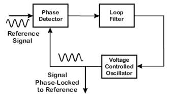
Fig. 1 Block diagram of a PLL system
III. Principle of operation
The system can visualized as a circuit accepting an input signal at some arbitrary frequency and providing an output signal of the same frequency which is not an exact copy of the input, but the output of an independent oscillator whose frequency is controlled by feedback. The output of the oscillator is compared to the input signal and if the frequencies are different, the frequency of the oscillator is altered so as to reduce the difference.
The phase detector compares the phases of its two input signals and provides an output signal that is proportional to their phase difference. The output of the phase detector is usually in the form of pulses that have to be filtered using the loop filter, and then applied to VCO. The polarities must be arranged so that if second signal lags the first signal, the VCO increases the frequency slightly; that is, the feedback must be negative. The output of the VCO is fed back to the phase detector, and hence the feedback loop is closed. Two of the most important specifications, namely, lock range and capture range that need to be kept in mind are defined as follows :
--Lock Range is the maximum frequency excursions over which the output remains locked with the input.
--Capture Range is the maximum difference between the input signals frequency and
oscillator's free running frequency where lock can eventually be attained.
IV. Types Of PLL
Although, broadly divided into the following four types, the PLLs can be of numerous types. The four main categories of PLLs are :
--Analog or Linear PLL (LPLL)
--Digital PLL (DPLL)
--All digital PLL (ADPLL)
--Software PLL (SPLL)
The one here presented is a digital PLL. Digital PLLs have emerged as the star players amongst all its other counterparts. It excels in frequency translation applications. In analog PLLs, the phase detector frequency can be kept high but at the expense of introduction of its own problems in the main circuit. In an analog PLL, low loop bandwidths require bulky loop filter components, which not only take up board space, but lead to self-resonance and microphonics when ceramic capacitors are used. The digital PLL also has shortcomings like a reference spur due to finite steps of phase correction, but this spur can be suppressed easily because the digital loop filter makes it easy to implement very small loop bandwidths (less than 1Hz). More importantly, because the loop characteristics are determined by digital coefficients, the loop dynamics are much more tightly-controlled than in an analog PLL. The loop parameters are programmable in a digital PLL, thus the user can maintain the same loop transfer function for a variety of desired conditions. The loop filter can be optimised for constant loop bandwidth and phase margin for both cases. More importantly, the loop parameters can be adjusted by merely programming registers instead of changing components, which has to be done whiling handling analog PLLs. Digital PLLs have the advantage of a high-speed DAC system clock for reference monitoring. This clock can be used to oversample the reference inputs, and allows for detection of reference clock drift or failure. Once a failure is detected, the device can either automatically switch inputs or go into hold-over mode. The stability of the output clock in holdover mode is the same as the stability of the system clock. The presence of DAC spurs is a potential drawback to digital PLLs. A low-pass reconstruction filter can eliminate these with considerable ease.
To overcome the limitations of either PLL design, it is possible to combine a digital PLL followed by an analog PLL. The digital PLL can handle clock switching and difficult frequency ratios, while the analog one can be used to further attenuate spurs, multiply to higher frequencies, and perform clock distribution.
A digital phase locked loop was presented for conventional applications. A model of the PLL suitable for time/frequency domain analysis was developed. The specifications and the characteristics of the PLL have been met. This model in its entirety was implemented in software. All the results are the simulations in the software and have been duly expressed.
V. Circuits used :
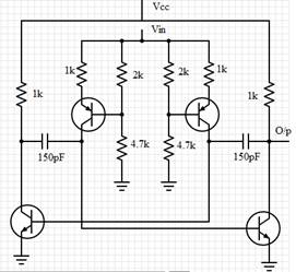
1. Voltage controlled oscillator(VCO) :
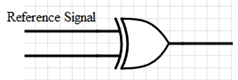
2. Phase detector :
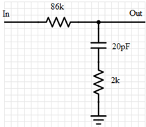
3. Loop filter :
VI. Output Waveforms:
1. VCO
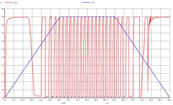
Where,
red represents input signal and blue represents output signal of VCO.
PHASE DETECTOR :
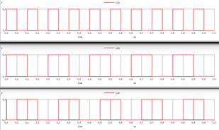
Where,
The upper two waveforms represent the input signals and the lower one represents the output signal.
LOOP FILTER :
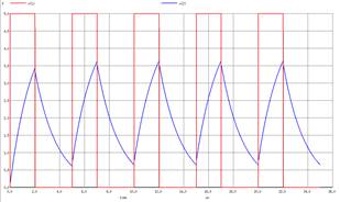
Where,
red represents input signal and blue represents output signal of loop filter.