Home > Digital CMOS Design > CMOS Inverter > Noise Margin
CMOS-Inverter
Noise Margin :
In digital integrated circuits, to minimize the noise it is necessary to keep "0" and "1" intervals broader. Hence noise margin is the measure of the sensitivity of a gate to noise and expressed by, NML (noise margin Low) and NMH (noise margin High).
NML and NMH are defined as,
NML = VIL VOL and NMH = VOH VIH
In order to define the terms VIL, VOL, VOH and VIH again consider the VTC of Inverter as shown in Figure below. The VOH is the maximum output voltage at which the output is "logic high". The VOL is the minimum output voltage at which the output is "logic low". The regions of acceptable high and low voltages are defined by VIH and VIL respectively. VIH and VIL represents the points where the gain dVoutdVin of VTC is equals to 1 as shown in above Figure. The region between VIH and VIL is called as the undefined region or transition width.
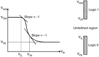
Fig2-Noise-Margin
Figure below shows the NMH and NML levels of two cascaded inverters. The noise margin shows the levels of noise when the gates are connected together. For the digital integrated circuits the noise margin is larger than '0' and ideally it is high.
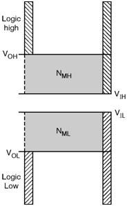
Fig2-Noise-Margin