Home > digital logic gates > nand gate
NAND Gate
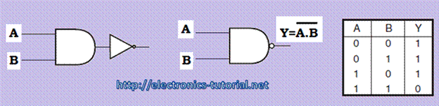
NAND stands for NOT AND. An AND gate followed by a NOT circuit makes it a
NAND gate Figure shows the circuit symbol of a two-input NAND gate. The
truth table of a NAND gate is obtained from the truth table of an AND gate
by complementing the output entries. The output of a NAND gate is a logic 0
when all its inputs are a logic 1. For all other input combinations, the
output is a logic 1. NAND gate operation is logically expressed as Y =
![]()
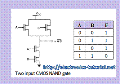
CMOS NAND Gate
The circuit below has two inputs and one output. Whenever at least one of the inputs is low, the corresponding PMOS transistor will be conducting while the NMOS transistor will be closed. Consequently, the output voltage will be high. Conversely, if both inputs are high, then both PMOS transistors at the top will be open circuits and both NMOS transistors will be conducting. Hence, the output voltage is low. The function of this gate can be summarized by the table. If logical 1's are associated with high voltages then the function of this gate is called NAND for negated AND. Again, there is never a conducting path from the supply voltage to ground.
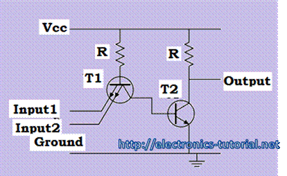
TTL NAND Gate
Circuit below shows the TTL implementation of NAND gate. Here, R1 and R2 are the pull-up resistors. VCC is the power supply. T1 is the bipolar junction transistor operated in totem pole configuration. T2 is the normal transistor.
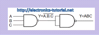
Three input NAND gate
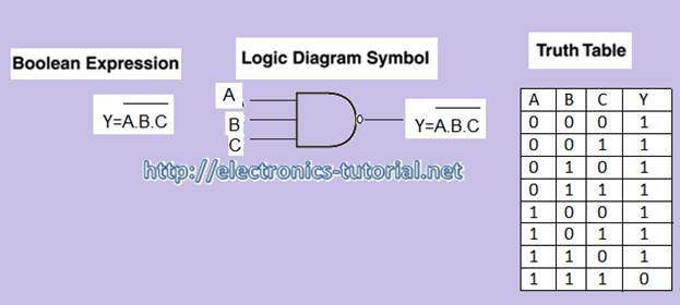
Figure above shows the three input AND gate. In this figure,
1) When the inputs A=0, B=0 and C= 0 then the output Y=1
2) When the inputs A=0, B=0 and C= 1 then the output Y=1
3) When the inputs A=0, B=1 and C= 0 then the output Y=1
4) When the inputs A=0, B=1 and C= 1 then the output Y=1
5) When the inputs A=1, B=0 and C= 0 then the output Y=1
6) When the inputs A=1, B=0 and C= 1 then the output Y=1
7) When the inputs A=1, B=1 and C= 0 then the output Y=1
8) When the inputs A=1, B=1 and C= 1 then the output Y=0
The Boolean expression for three input NAND gate and The truth table of the three input NAND gate is also shown in figure.
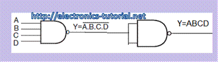
Four input AND gate
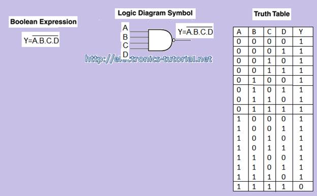
Figure above shows the four input AND gate. In this figure,
1) When the inputs A=0, B=0, C= 0 and D=0 then the output Y=1
2) When the inputs A=0, B=0, C= 0 and D=1 then the output Y=1
3) When the inputs A=0, B=0, C= 1 and D=0 then the output Y=1
4) When the inputs A=0, B=0, C= 1 and D=1 then the output Y=1
5) When the inputs A=0, B=1, C= 0 and D=0 then the output Y=1
6) When the inputs A=0, B=1, C= 0 and D=1 then the output Y=1
7) When the inputs A=0, B=1, C= 1 and D=0 then the output Y=1
8) When the inputs A=0, B=1, C= 1 and D=1 then the output Y=1
9) When the inputs A=1, B=0, C= 0 and D=0 then the output Y=1
10) When the inputs A=1, B=0, C= 0 and D=1 then the output Y=1
11) When the inputs A=1, B=0, C= 1 and D=0 then the output Y=1
12) When the inputs A=1, B=0, C= 1 and D=1 then the output Y=1
13) When the inputs A=1, B=1, C= 0 and D=0 then the output Y=1
14) When the inputs A=1, B=1, C= 0 and D=1 then the output Y=1
15) When the inputs A=1, B=1, C= 1 and D=0 then the output Y=1
16) When the inputs A=1, B=1, C= 1 and D=1 then the output Y=0
The Boolean expression for four input NAND gate and the truth table of the four input NAND gate is also shown in figure.
Form this analysis of AND gate we can see that,
1) For a two-input NAND gate, Output = (A.B)'
2) For a three-input NAND gate, Output = (A.B.C)'
3) For a four-input NAND gate, Output = (A.B.C.D)'
NAND gate as a Universal gate
The NAND is also known as universal gate. Because by using only NAND gate any kind of Boolean logic gate can be implemented. By using NAND gate we can easily implement the AND gate, OR gate and the NOT gate.
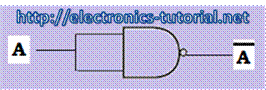
Implementation of NOT gate using NAND gate.
Figure below shows the implementation of the NOT gate using NAND gate. By shorting the two inputs of the NAND gate together the NOT gate can be implemented.
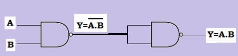
Implementation of AND gate using NAND gate.
Figure below shows the implementation of the AND gate using NAND gate. Here, by shorting the two inputs of the NAND gate together the NOT gate can be implemented. This implemented NAND when we will connect to the output of the NAND gate the AND gate will be implemented.
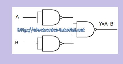
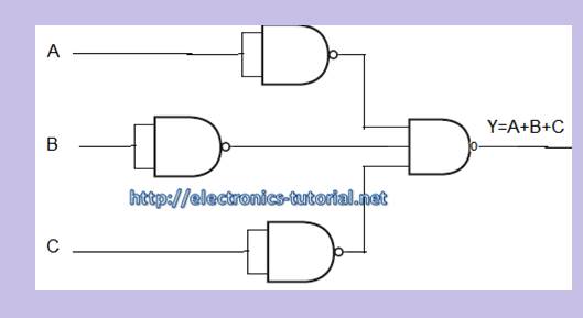
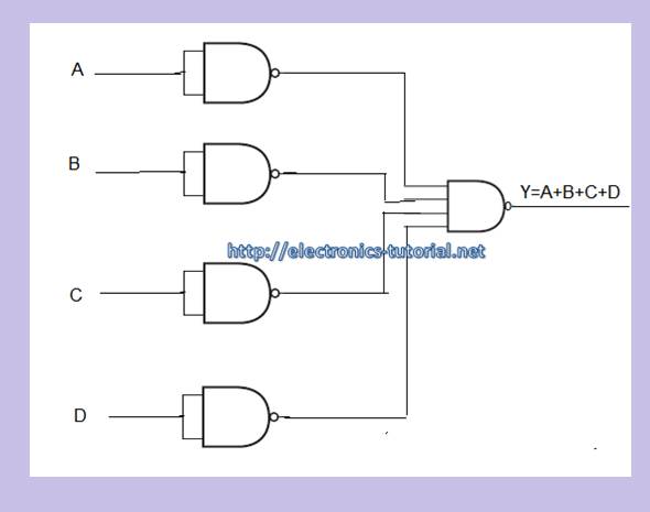
Implementation of OR gate using NAND gate.
Figure below shows the implementation of the OR gate using NAND gate. Here, by shorting the two inputs of the NAND gate together the NOT gate can be implemented. This implemented NAND when we will connect to the inputs of the NAND gate the OR gate will be implemented.
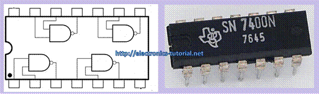
TTL NAND gate ICs
1) 7400 Quad 2-input NAND gate
2) 7410 Triple 3-input NAND gate
3) 7420 Dual 4-input NAND gate
4) 7430 Single 8-input NAND gate
CMOS NAND Gate ICs
1) 4011 Quad 2-input NAND gate
2) 4023 Triple 3-input NAND gate
3) 4012 Dual 4-input NAND gate