JTAG boundary scan, known as IEEE Standard 1149.1, is a testing standard. The advantage of this standard is to convert challenging problems in simple problems by using the software. The standard mechanism is to solve the problems. The standard defines instructions which are used in interconnect tests and built-in self tests. The top level schematic of the test logic defined by IEEE Std 1149.1 includes three key blocks that are TAP controller, Instruction register and Data registers. Figure below shows the block diagram of the JTAG architecture. It consists of boundry scan register, ID code register, user definable registers, Instruction register, TAP controller and Instruction decoder.
- TAP Controller :
The TAP controller responds to the control sequences through the test access port (TAP) and generates the clock and control signals for correct operation of other circuit blocks.
- Instruction Register :
The instruction register is a kind of shift register which is serially loaded with the instruction that selects an operation to be performed.
- Data Registers :
The data registers consists of the bank of registers created by using the shift register circuits. The stimuli used for the operation are loaded into the data registers and execution operation is started. Further, the results obtained after the execution are shifted for the testing.
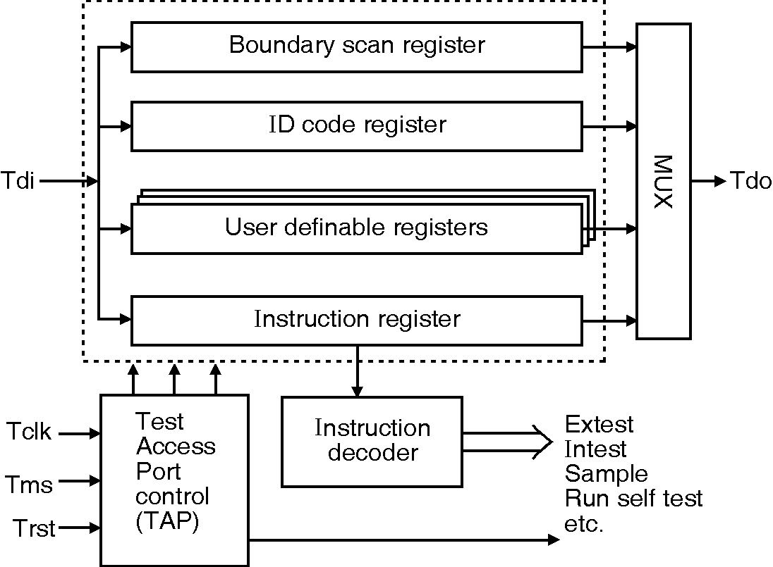
The TAP is a general-purpose port that can provide access to many test support functions built into a component, including the test logic defined by this standard. It is composed as a minimum of the three input connections and one output connection required by the test logic defined by this standard. An optional fourth input connection provides for asynchronous initialization of the test logic defined by this standard. The JTAG Test Access Port consists of four pins that drive the circuit blocks. The four pins, TMS, TCK, TDI and TDO.
TCK (Test Clock Input) : This pin sequences the TAP controller of the JTAG registers.
TMS (Test Mode Select Input) : This pin is the mode input signal that provides the control logic for JTAG.
TDI (Test Data Input) : This pin is the serial data input to all JTAG instruction and data registers.
TDO (Test Data Output) : This pin is the serial data output for all JTAG instruction and data registers.