Home > Analog CMOS Design > MOSFET Parasitics > Parasitic Capacitances MOSFETS
Parasitic Capacitances :
The schematic diagram of the MOSFET capacitances is shown in Figure below.
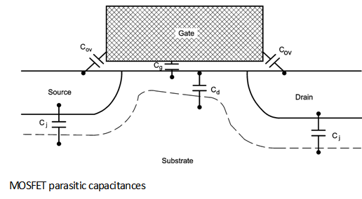
Here, along with Cg and Cd, parasitic capacitances such as, junction capacitance between the source or drain diffusion and the substrate and overlap capacitance between the gate and the source or drain region are present.
a) Junction capacitance (C j) :
The junction capacitances in a MOSFET is mainly due to the depletion charge between source/drain and the substrate.
Depending upon source/drain voltage the depletion charge changes. Further, when gate potential is larger than the threshold voltage the channel is created at the surface. Hence there is also existence of channel-to-substrate depletion capacitance.
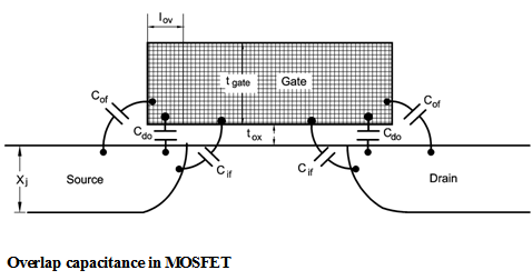
b) Overlap capacitance :
Another parasitic capacitance in MOSFET is the gate-to-source or gate-to-drain overlap capacitance.
It consists of three components : direct overlap, outer fringe and inner fringe as shown in Figure below. The direct overlap component simply can be written as,
Cdo = W ´ Iov ´ Cox
=
Where Iov is the length of the source or drain region under the gate. In the typical process, the oxide in the overlap region is somewhat thicker than tox due to bird's beak near the gate edge resulting from a reoxidation step. Therefore, Iov should be interpreted as equivalent overlap length, rather than an actual physical length.