Home > Digital CMOS Design > Pass Transistor Logic > Transmission Gate
Transmission-Gate | Pass-Transistor-Logic
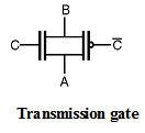
Transmission Gate Logic : The transmission gate logic is used to solve the voltage drop problem of the pass transistor logic. This technique uses the complementary properties of NMOS and PMOS transistors. i.e. NMOS devices passes a strong '0' but a weak '1' while PMOS transistors pass a strong '1' but a weak '0'. The transmission gate combines the best of the two devices by placing an NMOS transistor in parallel with a PMOS transistor as shown in Figure below. The control signals to the transmission gate C and ––C are complementary to each other. The transmission gate is mainly a bi-directional switch enabled by the gate signal 'C'. When C = 1 both MOSFETs are ON and the signal pass through the gate i.e. A = B if C = 1. Whereas C = 0 makes the MOSFETs cut off creating an open circuit between nodes A and B.

In this section CMOS logic circuits that are based on transmission gate are implemented. This indicates the use of transmission gate to implement logic circuits.
Basic Structure :
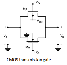
The basic structure of transmission gate is shown in Figure below which consists of NMOS and PMOS transistors. Here, VG is applied to NMOS, and (VDD- VG) applied to the PMOS.

The transmission gate work voltage-controlled switch. When VG is high, NMOS and PMOS are conducting hence switch is closed. Therefore, conduction path between left and right sides exist.
When VG is low, then the MOSFETs are in cutoff and switch is open. Therefore, there is no direct relationship between VA and VB.
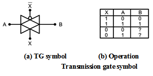
Figure below shows the symbol of transmission gate controlled by switching signals X and X* that are applied to the gates of NMOS and PMOS respectively.
