Home > Digital CMOS Design > MOS Capacitor > Band Diagram of Nonideal MOS with Bias
Band Diagram of Nonideal MOS Structure with Bias :
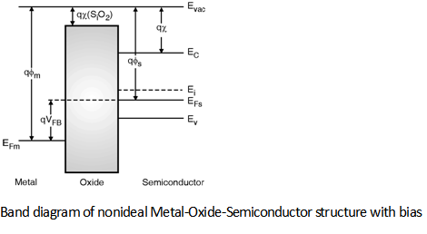
we have seen that because of the difference in the work function of both metal and semiconductor there is band bending at the surface of semiconductor.
In order to make the bands flat i.e. to remove the charges present there, the energy of the electrons to be lowered.
Hence, in order to lower the electron energy in the metal side a positive voltage VFB of magnitude Φm - Φs must be applied there. This is known as the flat band voltage of the MOS junction. and is given by,
VFB = Φm - Φs = Φms
The term Φms is known as work function difference of the metal semiconductor system. The band diagram of the nonideal MOS system after application of positive bias VFB is shown in Figure below. This diagram is also called as flat band diagram of the MOS structure.