Home > Digital CMOS Design > CMOS Inverter > VTC CMOS Inverter
VTC-CMOS-Inverter
Voltage Transfer Characteristics of CMOS Inverter : A complementary CMOS inverter is implemented using a series connection of PMOS and NMOS transistor as shown in Figure below. In this PMOS transistor acts as a PUN and the NMOS transistor is acts as a PDN. In order to plot the DC transfer characteristics graphically, I-V characteristics of NMOS and PMOS transistors are superimposed such graphical representation is called as a load line plot. It requires that the I-V curves of the NMOS and PMOS devices are transformed onto a common co-ordinate set.
Steps for Plotting Inverter DC Characteristics :
In order to plot the Inverter DC characteristics :
Let IDSn Drain current of NMOS transistor IDSp Drain current of PMOS transistor VTHn Threshold voltage of NMOS VTHp Threshold voltage of PMOS VDSn Drain to source voltage of NMOS VDSp Drain to source voltage of PMOS VGSn Gate to source voltage of NMOS VGSp Gate to source voltage of PMOS Vin Input voltage to inverter Vout Output voltage from inverter VDD DC bias applied to PMOS = 2.5 V
Step 1 : Write all the current and voltage relations for NMOS and PMOS transistors.
IINV = – IDSp = IDSn ; ...(a) VGSn = Vin 0 = Vin ; ...(b) VGSp = Vin VDD ; …(c) VDSn = Vout 0 = Vout ; ...(d) VDSp = Vout VDD …(e)
Step 2 : Transform IDSp Vs VDSp characteristics into IDSn Vs VDSp characteristics using Equation.
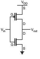
Fig1-VTC-CMOS Inverter
Step 3 : Transform VGSp into Vin in the IDSn Vs VDSp characteristics using Equation
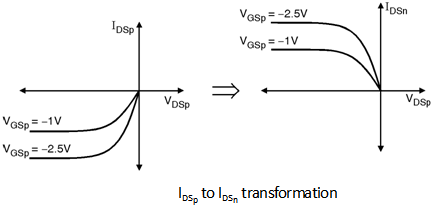
Fig2-VTC-CMOS Inverter
Step 4 : Transform VDSp into Vout in the IDSn Vs VDSp characteristics using Equation
Vout = VDD + VDSp .
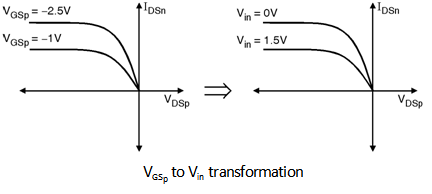
Fig3-VTC-CMOS Inverter
Step 5 : Merge IDSn Vs VDSn i.e. IDSn Vs Vout characteristics of NMOS and the IDSn Vs Vout characteristics transformed in step 4. (Refer Equation (7.5.1(d)).
For the dc operating points the currents through the NMOS and PMOS devices must be equal and from the below Figure these points are for Vin = 0, 0.5, 1, 1.5, 2 and 2.5 V at these input voltages the IDSn = IDSp and these are the intersecting points of both IDSn Vs Vout and IDSp Vs Vout (i.e. transformed to IDSn Vs Vout) characteristics.
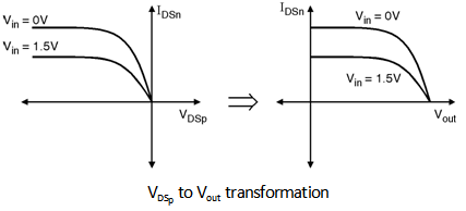
Fig4-VTC-CMOS Inverter
From these points now we can plot the voltage transfer characteristics as shown in below Figure with various regions.
Before addressing the VTC in detail let us discuss the various operating modes of NMOS and PMOS transistors with respect to the applied input voltage these results are tabulated as shown in Table below.
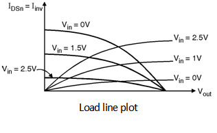
Fig5-VTC-CMOS Inverter
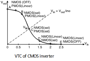
Fig6-VTC-CMOS Inverter
The VTC of complementary CMOS inverter is as shown in above Figure. The characteristics are divided into five regions of operations discussed as below :
Region A :
In this region the input voltage of inverter is in the range 0 Vin VTHn. Hence the NMOS is in cut-off and PMOS is in linear region and output voltage is VDD.
Region B :
In this region VTHn Vin < VDD2 in which p device is in linear region and n device is in saturation.
The current for PMOS operated in linear mode is given by, i.e. IDSp = p Cox WLp (VGSp VTHp) VDSp VDSp22 …(7.5.2) Interms of Vin and Vout it is given as : IDSp = p Cox WLp (Vin VDD VTHp) (Vout VDD) (Vout VDD)22 …(7.5.3) The term p Cox WLp is also represented by p called as gain factor of PMOS transistor. Also, the current for NMOS transistor operated in saturation mode is given by, i.e. IDSn = 12 n Cox WLn (VGSn VTHn)2 IDSn = 12 n Cox WLn (Vin VTHn)2 …(7.5.4)
Also, the factor n Cox WLn is also represented by n called as gain factor of NMOS transistor.
Region C : This region is shown at the middle of the transition curve of VTC. In this region both the NMOS and PMOS transistor are operated in saturation region. The saturation current for both the transistor is given by, IDSn = 12 n Cox WLn (VGSn VTHn)2 = 12 n Cox WLn (Vin VTHn)2 …(7.5.5) and IDSp = 12 p Cox WLp (Vin VDD VTHp)2 …(7.5.6)
Region D :
This region is characterized by VDD2 < Vin VDD + VTHp In this region PMOS transistor is in saturation and the NMOS transistor is operated in linear region.
The current through NMOS transistor is given as :
IDSn = n Cox WLn (Vin VTHn) Vout (Vout2)2 …(7.5.7)
The current through PMOS transistor is given as :
IDSp = 12 n Cox WLp (Vin VDD VTHp)2 …(7.5.8)
Region E :
This region is described by the input voltage in the range Vin VDD VTHp. In this region PMOS transistor is OFF and the NMOS transistor is in linear mode. The output voltage in this region Vout = 0. From the detailed analysis of VTC characteristics it can be observed that, CMOS inverter has a very narrow transition zone. Therefore, high gain can be achieved when both NMOS and PMOS are simultaneously ON and operated in saturation. Thus, in transition region a small change in the input voltage results in a large output variations.