Home > mini projects > VOLTAGE REGULATOR
Abstract -The aim of the project is to design a low cost voltage regulator with the following specifications: 1) A fixed output voltage in the range of 2 to 7 Volts, 2) Input Voltage Range 9 to 40 Volts, 3) Low output current in mA, and 4) Short Circuit Protection. It is a series type of linear voltage regulator.
I. INTRODUCTION
A voltage regulator is a voltage stabilizer that is designed to automatically stabilize a constant voltage level. A voltage regulator circuit is also used to change or stabilize the voltage level according to the necessity of the circuit. Thus, a voltage regulator is used for two reasons:-
1. To regulate or vary the output voltage of the circuit.
2. To keep the output voltage constant at the desired value in-spite of variations in the supply voltage or in the load current.
Voltage regulators find their applications in computers, alternators, power generator plants where the circuit is used to control the output of the plant. Voltage regulators may be classified as electromechanical or electronic. It can also be classified as AC regulators or DC regulators.
In general, these regulators can be divided into several classes:
- Linear series regulators
- Switching regulators
Series Regulators use a power transistor connected in series between the unregulated DC input and the load. The output voltage is controlled by the continuous voltage drop taking place across the series pass transistor. Since the transistor conducts in the active or linear region, these regulators are also called linear regulators. Linear Regulators may have fixed or variable output voltage and could be positive or negative.
Switching regulators on the other hand, operate the power transistor as a high frequency on/off switch, so that the power transistor does not conduct current continuously. This gives improved efficiency over series regulator.
|
II. |
CIRCUIT DIAGRAM |
||||||||||
|
R3 |
|||||||||||
|
VCC |
1kΩ |
VCC |
|||||||||
|
12V |
C2 |
||||||||||
|
D1 |
12V |
||||||||||
|
1N4737A |
7 |
1 |
5 |
U1 |
100pF |
Q1 |
XMM1 |
||||
|
3 |
|||||||||||
|
6 |
2N2222A |
||||||||||
|
I1 |
|||||||||||
|
2 |
4 |
U2 |
R4 |
||||||||
|
R1 |
|||||||||||
|
10uA |
|||||||||||
|
4 |
741 |
2kΩ 2 |
100Ω |
||||||||
|
0kHz |
6 |
Q2 |
D2 |
||||||||
|
0° |
|||||||||||
|
1N4737A |
|||||||||||
|
3 |
|||||||||||
|
2N2222A |
|||||||||||
|
R2 |
7 |
1 |
5 |
741 |
|||||||
|
3kΩ |
VCC |
||||||||||
|
12V |
|||||||||||
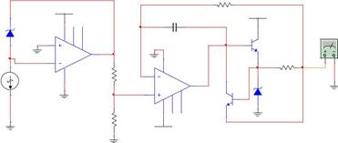
WORKING:
The zener diode, a constant current and reference amplifier produce a fixed voltage of about 7 Volts at Terminal Vref.
The constant current source forces the zener to operate at a fixed point so that, the zener outputs a fixed voltage.
The circuit also consists of an error amplifier, a series pass transistor Q1 and a current limit transistor Q2. The error amplifier compares a sample of the output voltage applied at the Inv input terminal to the reference voltage Vref, applied at the NI input terminal. The error signal controls the conduction of Q1.
The voltage at the NI terminal of the error amplifier due to R1,R2 divider is
VNI = Vref x (R2/R1+R 2)
The difference between VNI and Vo (Output Voltage) which is directly fed back to INV terminal, is amplified by error amplifier. The output of the error amplifier drives the pass transistor Q1, so as to minimize the difference between the NI and INV inputs of error amplifier. Since Q1 is operating as an emitter follower,
Vo = Vref x (R2/R1+R 2)
If the output voltage becomes low, the voltage at the INV terminal of error amplifier also goes down. This makes its output to become more positive, there by driving Q1 more into conduction. This reduces the voltage across Q1 and drives more current into the load causing voltage across load to increase. So the initial drop in the load voltage has been compensated. Similarly any increase in load voltage or changes in the input voltage get regulated.
To protect the circuit we provide a current limit facility. Current limiting refers to the ability of a regulator to prevent the load current from increasing above a present value.
The current limit is set by connecting an external resistor R4 between the emitters of Q1 and Q2.
The load current produces a small voltage drop V4 across R4. This voltage V4 is applied directly across the base emitter junction of Q2. When this voltage is approximately 0.5 V, Q2 begins to turn on, now a part of current from error amplifier, goes to the collector of Q2, there by decreasing the base current of Q1. This in turn reduces the emitter current of Q1. So any increase in load current will get nullified. Similarly if the load current decreases Vbe of Q2 drops repeating the cycle in such a manner that the load current is held constant to produce a voltage across R4 sufficient to turn ON Q2. This voltage is typically 0.5 Volts.
Ilimit = V4/R4.
This method of current limiting is also referred to as Current Sensing Technique.
A. CODE
.subckt OPAMP 1 2 6
R1 1 2 10meg
R2 3 4 1k
E1 3 0 2 1 100k
C1 4 0 15u
E2 5 0 4 0 1
R3 5 6 10
.ends OPAMP
*Voltage Regulator
.include opamp_symbol.cir
.model 1N4737a D( IS =5.038e-012 BV=7.165 IBV=0.1902 EG=1.11 TNOM=27)
.model 2N2222A npn(IS=2.04566e-13 BF=300)
D1 1 2 1N4737a
I 1 0 10u
X1 1 0 2 opamp
R1 2 3 0.38k
R2 3 0 1k
Vcc 8 0 15V dc
X2 4 3 5 opamp
R3 4 6 100
R4 7 6 100
Rl 6 9 1k
V2 9 0 dc 0V
C1 4 5 100p
D2 0 7 1N4737a
Q1 8 5 7 2N2222A
Q2 5 7 6 2N2222A
.tran 1u 1m
.control
run
display
plot V(2)
plot V(6)
plot I(V2)
set color0 = white
set color1 = black
.endc
.end
*Load Regulation - Output Voltage variation with respect to current load variation
.include opamp_symbol.cir
.model 1N4737a D( IS =5.038e-012 BV=7.165 IBV=0.1902 EG=1.11 TNOM=27)
.model 2N2222A npn(IS=2.04566e-13 BF=300)
D1 1 2 1N4737a
I 1 0 10u
X1 1 0 2 opamp
R1 2 3 2k
R2 3 0 3k
X2 4 3 5 opamp
R3 4 6 100
R4 7 6 100
Rl 6 9
V2 9 0 dc 0V
C1 4 5 100p
D2 0 7 1N4737a
Q1 8 5 7 2N2222A
Q2 5 7 6 2N2222A
.dc Rl 1k 10k 100
.control
run
display
plot V(2)
plot V(6)
plot I(V2)
plot V(7)
plot V(6) Vs I(V2)
set color0 = white
set color1 = black
.endc
.end
RESULT AND CONCLUSION

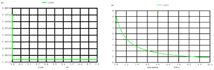
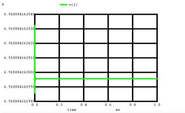
Reference voltage is set to obtain 6.91v and hence output
voltage is obtained in range of 2v-7v changing resistances.
V(2) is output voltage of the voltage regulator which is
observed to be constant 5v for resistances 0.38kohm and
1kohm.
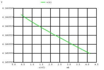
Current at node 2 is observed to be 5mA. When the output resistance is varied from 1k to 10k, current is observed to vary from 4mA to 0.5mA. Output voltage is varied from 4.145v to 4.146v on varying current 0 to 4mA.