Home > mini projects > MOSFET driver circuit to interface MOSFETs with microcontroller for high speed application
MOSFET driver circuit to interface MOSFETs with microcontroller for high speed application
Abstract -Modern day gadgets which use Brushless motors for extremely high speed application make use of Electric Speed Controller (ESC), which is a circuit to drive the BLDC motors by converting DC voltage into an equivalent of a 3 phase AC voltage with the help of very fast switching mosfets, and microcontroller to control their switching . This project describes the design of a circuit suitable for high speed switching application and focuses on the configurational elements for fine tuning of this circuit for a particular application.
I. INTRODUCTION
T HE use of Electronic Speed Controllers are increasing rapidly due to the increasing popularity of Quadcopters, Electric Skateboards and similar gadgets. Electronic industry is rapidly increasing in both High power technology as well as low power technology, as a result the high power circuits like MOSFETs capable of driving 240 Amperes of current at 60V and at the same time the low power circuits are operating at 3.3v suppling 200mA or lesser at output pins. Interfacing of these 2 component in same circuit gives rise to certain problems. This project focuses on describing in detail the
problems and suggesting suitable solutions for them.
II. PROBLEMS WITH HIGH POWER MOSFETS
MOSFETs are basically charge controlled devices, charge at gate terminal dictates the ability of MOSFET to flow current between Drain and Source. Thus, Gate of MOSFET can essentially be treated as a capacitance whose charge is the controlling factor in the operation of the MOSFET. This capacitance nature leads to some problems especially at higher power levels these are described below
A. Higher capacitances leads to large propagation delays
As the gate needs to store charge for controlling the operation of MOSFET, the storing of charge takes some finite time. As the input voltage reduces, the time required for the charging of capacitor also increases. Furthermore, if the
This work was supported by Dr. Ganesh Patil, Electronics and Communication Engineering Department, VNIT Nagpur as a project report for NGSPICE simulation of MOSFET Driver circuit
current provided or supplied is restricted by the current sourcing or sinking capabilities of microcontroller or microprocessor, then the switching time further increases creating an increased level of problem.
B. Reduced Noise immunity
The most common method for reducing the effect of high frequency low voltages noise is to add a low-pass filter which is most conveniently done by adding a Resistor-Capacitor (RC) network which is also quite effective. But as adding capacitance further increases the switching time, it is not recommended for higher power applications
III. SOLUTION FOR HIGHER POWER MOSFETS
The problems mentioned in section II can easily be solved by adding an interfacing circuit intermediate between low power elements and High power elements. This circuit in this particular application can be a MOSFET driver circuit. MOSFET driver circuits are most commonly made by using MOSFETs or/and Insulated Gate Bipolar Transistors (IGBT). The choice between these two basically is made by taking into consideration the power dissipation in these two elements during their operation. Usual choice for voltage under 250 volts is MOSFET drivers using MOSFETs. In the range of 250 to 1000 Volts, the choice is application specific. Above 1000V the choice is definitely IGBTs as they tend to dissipate less power than MOSFETs at higher voltages
A. Solution for decreasing switching time
MOSFET drivers have capabilities to supply high voltages and can source a lot more current than microcontrollers which significantly increases the switching speed of the target MOSFET and also at the same time have small gate capacitances which increases there speed too. Thus overall the whole process of switching becomes a lot faster than without using the driver circuitry.
B. Solution to increase noise immunity
The capacitance can't be added to reduce the noise as it would increase the switching time and hence we need a circuit which has least capacitive nature and also it can reduce the effects of noise. One such circuit is Schmitt trigger circuit. Schmitt trigger basically uses different voltage reference levels for switching from high to low and from low to high and thus all the noise in between these 2 voltage levels are just
removed and hence the noise immunity increases tremendously without any addition in switching time which is obviously what we needed. The practical implementation is done by adding an inverter with inbuilt Schmitt trigger and another inverter in series with it to nullify its inverting effect but still the noise reduction capability. The inverter with inbuilt Schmitt trigger is made by using total of six MOSFETs, three PMOS and three NMOS MOSFETs. There particular arrangement is shown in Fig 1

Fig. 1. Schmitt trigger circuit using CMOS technology. This is a inverter circuit with inbuilt Schmitt trigger
Referring to figure 1, we can explain the working of Schmitt trigger. Consider Vin to be 0V, then Q4 and Q6 transistors will be ON and Output will be HIGH thus switching Q3 ON and thus making source voltage at Q1 close to Vcc. Now when the Vin becomes greater than threshold voltage of NMOS, Q2 turns ON giving rise to a voltage divider network between Q3 and Q2 and makes source voltage of Q1 to be Vcc/2 and thus the switching occurs at Vcc/2 + Vth1, where Vth1 is threshold voltage of NMOS. This was switching from High to Low, now when switching from Low to High similar actions take place at PMOS side and voltage reference becomes Vcc/2-Vth2 where Vth2 is the threshold of PMOS and thus the reference voltages at 2 different transactions are different, providing a higher noise immunity to the whole circuit.
IV. CIRCUIT EXPLANATION
Circuit Diagram is shown in the Fig 2. Circuit can be divided vertically ion 3 parts for easy explanation. Part A contains elements to the left of U2 inverter, Part B contains
Fig. 2. MOSFET driver circuit diagram

elements in between U2 and U3 and part C contains elements to the left of U3.
Part A is basically the noise simulation and its removal by using Schmitt trigger. The voltage source with high frequency signal represents the simulated noise. Inverter with some slanted hysteresis symbol U1 represents the inverter with inbuilt Schmitt trigger. And U2 is placed to remove the inversion due to Schmitt triggered inverter.
Part B contains the additional circuit to control the threshold voltage of the switching of circuit. The current source is the biasing circuit for transistor Q2 and thus by controlling the current parameters we can make changes in the circuit for changing the voltage levels of the circuitry.
Part C is another inverter at output side using CMOS circuit so as to offer high impedance to the circuit following the MOSFET driver which most probably will be another MOSFET.
V. SIMULATION RESULTS
In Fig 3 we see the output of an inverter without Schmitt trigger and its corresponding output with Schmitt trigger which clearly shows the additional noise immunity presented by Schmitt trigger.
In Fig 4 we see the final results in which a high voltage output is produced as the final output of the MOSFET driver circuit.
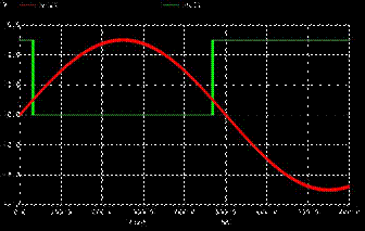
In Fig 5 we can see the effect of changing the bias current of MOSFET Q2. In (A) the current is 50uA and in (B) the current is reduced to 10uA and the results are clearly visible. The decreasing of current has reduced the threshold levels.
Fig 3. Effect of Schmitt trigger
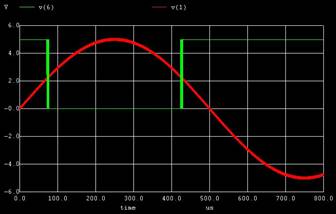
(A) Without Schmitt Trigger
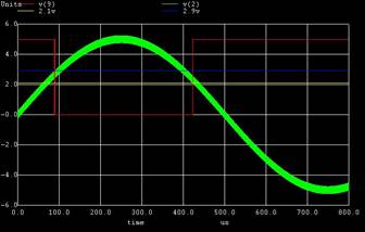
(B) With Schmitt Trigger Fig 4. Final Output
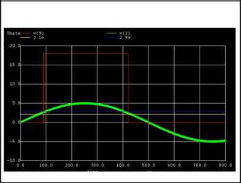
Fig 5. Effect of changing biasing current

(A) I = 50uA

(B) I = 10uA
VI. CONCLUSION
After Studying the Simulation circuits we can clearly see the effect of each MOSFET driver element on the output of the circuit. Hence we conclude that we can fine tune this circuit according to our needs by changing the parameters of this circuit. This MOSFET circuit is highly efficient, fast and extremely robust against the noise