The XC9500 CPLD has the facility of in-system programming and also includes the testing facility. The devices in this series have around ten thousand programm erase cycles. The XC9500 family is fully pin-compatible with Enhanced pin-locking capability. It has Expanded JTAG instruction set. The block diagram of XC9500 family is shown in figure below, XC9500 consists of multiple function blocks and I/O blocks, The Input/Output Block provides buffering for device input and output. The function block provides programmable logic capability.The FastCONNECT II switch matrix connects all function blocks. The function block consists of 18 macro cells capable of implementing a combinational and sequential logics. The function block receives global clock, output enable and their corresponding output enable signals also drive the IOB. The function block generates 18 outputs for driving the Fast CONNECT switch matrix. The logic is implemented in SOP form. Macrocell is made up of logic circuits. Macro cells contain arithmetic logic unit for arithmetic functions. Product terms from the AND-array are present in macrocell for primary data inputs. The main application of product term allocator is to control the product terms. To increase the logic capacity of a macrocell product term allocator is used in the function block. The FastCONNECT switch matrix connects signals to the function block inputs. The input/output block outputs and function block outputs drive the FastCONNECT matrix. Input/Output Block is the interface between internal logic and the Input/Output pins. The Input/Output block contains input buffer, output driver, output enable selection multiplexer, and user programmable ground control. The Input/Output Block provides slew-rate control. The Input/Output Block provides user programmable ground pin capability.
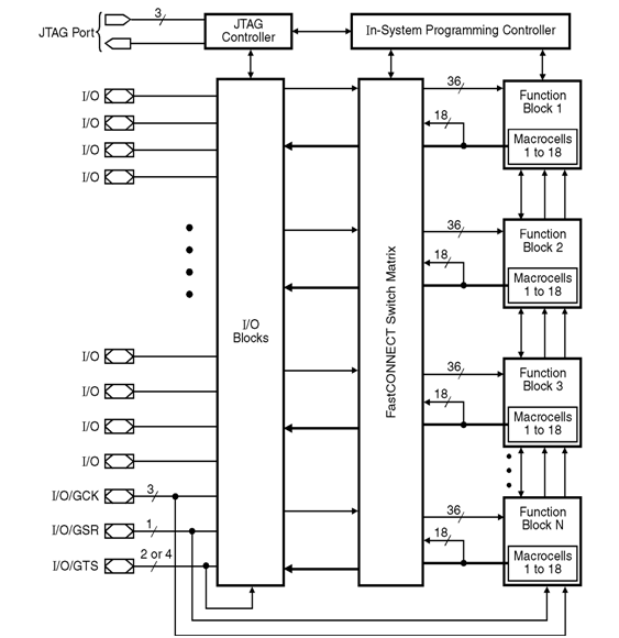 Fig_XC9500 CPLD Family