Need of Design for Testability
Recently, the semiconductor industry is changing on various aspects such as,
- Smaller features on silicon
- Reduction in voltages
- Development of new fabrication techniques
- Complex macrocells
- Reuse of existing complex macrocells
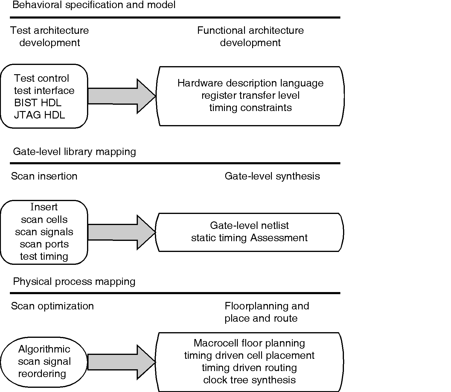
These industry changes requires quality and reliability. Therefore, to place large logic and memory on a single die the cost increases. Figure below shows various levels of VLSI design flow. The key optimization factors are,
1) Amount of vector data,
2) Complexity of the tester,
3) Timing management.
In the industry when the faulty integrated chips pass thorough the improper test, the system failures and larger difficulty in system debugging are found. In this view the debugging cost increases ten times from chip level to board level and also from board level to system level. Therefore, it is of necessary to detect faults as early as possible. Further, as the number of transistors integrated into a chip increases, the task of chip testing to detect the faults and check the functionality becomes more difficult. The complexity in the manufacturing process of die on a wafer is increasing day by day. Small imperfections in starting material, processing steps, or in photomasking results in bridged connections or missing features. In order to determine which die are good and should be used in end systems test procedure plays an important role.