Home > Analog CMOS Design > MOSFET Fundamentals > Linear Region of Operation
Linear Region of Operation :
Consider a n-channel MOSFET whose terminals are connected as shown in Figure below assuming that the inversion channel is formed (i.e. V GS > VTH) and small bias is applied at drain terminal.
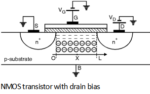
Now suppose the drain voltage is greater than zero. As the channel potential varies from '0' at the source to the VD at the drain, current IDS starts flowing from the drain to source because of this potential difference.
The local voltage difference between gate and channel now varies from V G to VG - VD. Thus the charge density at point 'x' along the channel can be written as
Qi (x) = - Cox [VGS - V (x) - V TH]
Where V (x) is the channel potential at 'x' and
Cox = is the oxide capacitance
with Îox = 3.9 ´ Îo = 3.5 ´ 10- 11 F/m and tox is the oxide thickness.
IDS = - nn (x) × Qi (x) W
The electron drift velocity is related to the electric field through a parameter called mobility (mn) as :
nn = - mn E (x)
But the electric field E (x) can be expressed as :
E (x) = -
\ nn (x) = mn
Substituting Equations (8.3.10) and (8.3.6) in Equation (8.3.7) we get,
IDS = W Cox mn [VGS - V (x) - V TH] ×
i.e. IDS × dx = mn Cox W [VGS - V (x) - VTH] dV (x)
By using the Boundary conditions,
i.e. V (O) = 0 and V (L) = VDS
and integrating the Equation over the length of channel 'L' we get,
IDS × dx = mn Cox W [VGS - V (x) - V TH] × dV (x)
Assuming mobility (mn) and threshold voltage (VTH) constant over 'x' we get,
IDS = mn Cox
Here the product of mn and Cox is called as the process transconductance parameter given as :
Kn¢ = mn Cox =
The product of process transconductance (Kn¢) and the ratio of an transistor is called as the gain factor (Kn) given as :
Kn = Kn¢ × = mn Cox
Therefore the drain to source current equation becomes :
IDS = mn Cox = Kn¢
= Kn
The operating region where Equation holds is called as resistive or linear region of operation.
The important point here to note that 'L' is the effective channel length.
The ID - VDS relation given by Equation represents a parabola which is plotted as shown in Figure below shows for various values of VGS and indicates that the current capability of device increases with VGS.
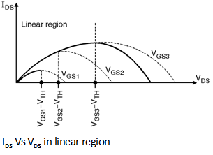
By calculating and equating to zero, we get that the peak of each parabola occurs at VDS = VGS - VTH and the peak current is,
IDSmax = mn Cox (VGS - V TH)2
The difference (VGS - VTH) is called as the “overdrive voltage†and the ratio is called as the “aspect ratioâ€. If V DS £ (VGS - VTH) then the device is said to be operate in triode region.
If in Equation , VDS << 2 (VGS - VTH ),
We have, IDS » mn Cox (VGS - V TH) VDS
i.e. The drain to source current is a linear function of VDS for small values of VDS and each parabola from above Figure can be approximated by a straight line. The linear relationship implies that the path from the source to the drain can be represented by a linear resistor given as :
Ron =
Thus a MOSFET can be operated as a resistor whose value is controlled by overdrive voltage (VGS - VTH).