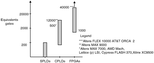
In all the Programmable logic devices the first Programmable logic devices developed is the Programmable Read-Only Memory. In Programmable Read-Only Memory the input provided to the digital circuit are worked as the address lines and the outputs of the digital circuit are worked as a data lines. Thus PROM is an inefficient Programmable logic device for the logic circuits. The first device developed for implementing the logic circuits is the Field-Programmable Logic Array (FPLA), which is simply called as PLA. PLA consists of two levels of logic gates, a programmable AND-plane followed by a programmable OR-plane. In PLA the inputs are logically AND together in AND-array and each AND-array output correspond to the product term of the inputs. Further, each OR-array output is configured to produce the logical sum of any of the AND-array outputs. PLAs are used to implement logic functions in sum-of-products form. Figure below shows the categories of PLDs indicating the logic capacities available in each of the three categories. In simple Programmable logic device architecture the main problem is the requirement of the programmable logic-planes. Many commercial PLD products are available in the market with the basic structure are known as complex Programmable logic device (CPLDs). The largest capacity general purpose chips are the Mask-Programmable Gate Arrays (MPGAs). The MPGAs are nothing but the array of transistors which forms the logic circuit with the help of custom connecting interconnect. Although MPGAs are not in the category of programmable logic devices they are used to in Field- Programmable Gate Arrays (FPGA).
 Fig_Evolution of Programmable logic devices