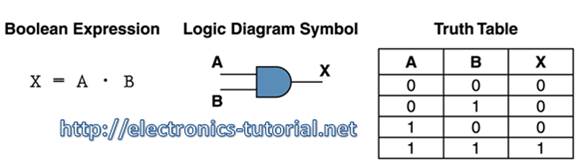
An AND gate is a logic gate in which two or more inputs and one output is present. The output of an AND gate is HIGH only when all the inputs are in the HIGH state. In all other cases, the output is LOW. The output of the AND gate is a logic 1 only when all of its inputs are in logic 1 state. In all other cases, the output is logic 0. The logic symbol and truth table of a two-input AND gate are shown in Figure. The AND operation on two independent logic variables A and B is written as X = A.B. Here, A and B are input logic variables and X is the output.
Wired AND gate:
A wired logic connection is a logic gate that implements Boolean logic using only passive components such as diodes and resistors. A wired logic connection can create an AND gate. The wired AND connection uses a pull up resistor and one diode per input to create this function. The positive voltage from the source is directed away from the output through diodes connected directed towards the inputs. When positive logic that is equal to or greater than that of the source is applied to all inputs the source voltage is directed to the output. The AND gate is capable of an arbitrary number of inputs. Figure below shows the wired AND gate circuit.
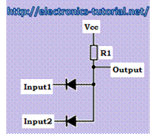
Figure above shows the wired AND gate circuit. It consists of two diodes and the one pull-up resistor.
1) When Input1=0 and Input2=0 both the diodes are ON. Therefore, output short circuited to Input1 and the output is also short circuited to Input2. Therefore, since both Input1 and Input2 are at logic 0. The output =0.
2) When Input1=0 and Input2=1 one diode is which is connected to Input1 is ON and the other diode which is connected to Input2 is OFF. Therefore, output is short circuited to Input1 and the output is open circuited to Input2. Therefore, Since Input1=0 and Input2 =1. The output =0.
3) When Input1=1 and Input2=0 one diode is which is connected to Input1 is OFF and the other diode which is connected to Input2 is ON. Therefore, output is open circuited to Input1 and the output is short circuited to Input2. Therefore, Since Input1=1 and Input2 =0. The output=0.
4) When Input1=1 and Input2=1 one diode is which is connected to Input1 is OFF and the other diode which is connected to Input2 is OFF. Therefore, output is open circuited to Input1 and the output is open circuited to Input2. Therefore Since Input1=1 and Input2 =1. The output =1. This is mainly the voltage drop across the pull-up resistor connected as shown in figure.
CMOS AND gate
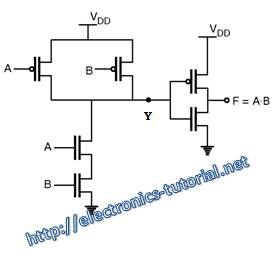
Figure above shows the CMOS implementation of the two input AND gate. It consists of NMOS and PMOS transistors.
1) When A=0 and B=0 both the PMOS transistors are on and both the NMOS transistors are OFF Therefore the output Y is logic 1. As the Y is connected to the input to the CMOS inverter the output F is at logic 0
2) When A=0 and B=1 then the PMOS transistor which is connected to the A input is on and the PMOS transistor which is connected to the B input is OFF. Further, the NMOS transistor which is connected to the A input is OFF and the NMOS transistor which is connected to the B input is ON. Therefore, the output Y is logic 1. As the Y is connected to the input to the CMOS inverter the output F is at logic 0.
3) When A=1 and B=0 then the PMOS transistor which is connected to the A input is OFF and the PMOS transistor which is connected to the B input is ON. Further, the NMOS transistor which is connected to the A input is ON and the NMOS transistor which is connected to the B input is OFF. Therefore, the output Y is logic 1. As the Y is connected to the input to the CMOS inverter the output F is at logic 0.
4) When A=1 and B=1 both the PMOS transistors are OFF and both the NMOS transistors are ON Therefore the output Y is logic 0. As the Y is connected to the input to the CMOS inverter the output F is at logic 1.
AND gate using BJTs
Figure below shows the implementation of the two input AND gate using bipolar junction transistors. It consists two bipolar junction transistors. These transistors are work as a switches. These switches are connected in series
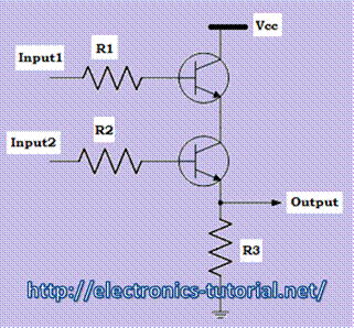
1) When input1=0 and Input2=0 both the transistors are OFF. Therefore the output is logic 0.
2) When input1=0 and Input 2=1 then the transistor which is connected to the input1 is OFF and the transistor which is connected to the input2 is ON. Therefore, the output is logic 0.
3) When input1=1 and Input 2=0 then the transistor which is connected to the input1 is ON and the transistor which is connected to the input2 is OFF. Therefore, the output is logic 0.
4) When input1=1 and Input 2=1 then the transistor which is connected to the input1 is ON and the transistor which is connected to the input2 is ON. Therefore, the output is logic 1.
Three input AND gate
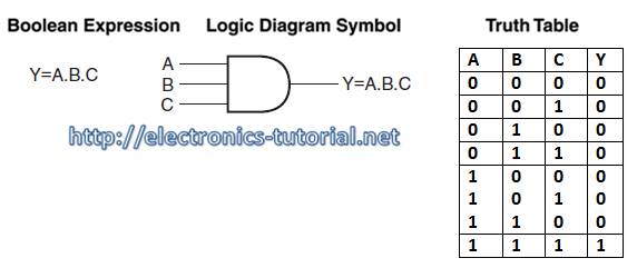
Figure above shows the three input AND gate. In this figure,
1) When the inputs A=0, B=0 and C= 0 then the output Y=0
2) When the inputs A=0, B=0 and C= 1 then the output Y=0
3) When the inputs A=0, B=1 and C= 0 then the output Y=0
4) When the inputs A=0, B=1 and C= 1 then the output Y=0
5) When the inputs A=1, B=0 and C= 0 then the output Y=0
6) When the inputs A=1, B=0 and C= 1 then the output Y=0
7) When the inputs A=1, B=1 and C= 0 then the output Y=0
8) When the inputs A=1, B=1 and C= 1 then the output Y=1
The Boolean expression for three input AND gate is Y= A.B.C. The truth table of the three input AND gate is also shown in figure.
Four input AND gate
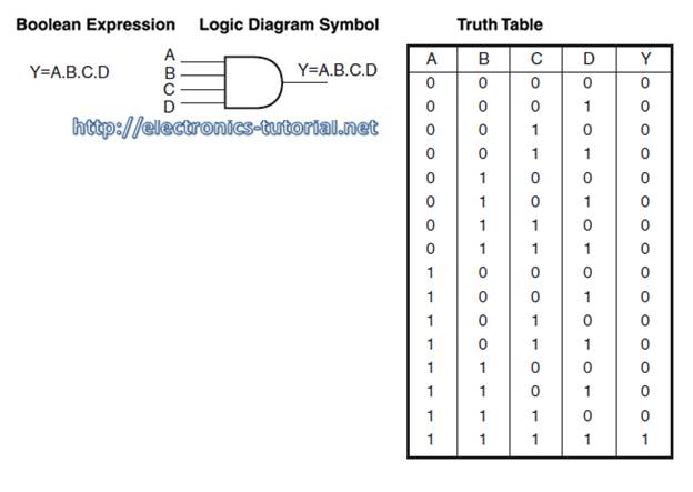
Figure above shows the four input AND gate. In this figure,
1) When the inputs A=0, B=0, C= 0 and D=0 then the output Y=0
2) When the inputs A=0, B=0, C= 0 and D=1 then the output Y=0
3) When the inputs A=0, B=0, C= 1 and D=0 then the output Y=0
4) When the inputs A=0, B=0, C= 1 and D=1 then the output Y=0
5) When the inputs A=0, B=1, C= 0 and D=0 then the output Y=0
6) When the inputs A=0, B=1, C= 0 and D=1 then the output Y=0
7) When the inputs A=0, B=1, C= 1 and D=0 then the output Y=0
8) When the inputs A=0, B=1, C= 1 and D=1 then the output Y=0
9) When the inputs A=1, B=0, C= 0 and D=0 then the output Y=0
10) When the inputs A=1, B=0, C= 0 and D=1 then the output Y=0
11) When the inputs A=1, B=0, C= 1 and D=0 then the output Y=0
12) When the inputs A=1, B=0, C= 1 and D=1 then the output Y=0
13) When the inputs A=1, B=1, C= 0 and D=0 then the output Y=0
14) When the inputs A=1, B=1, C= 0 and D=1 then the output Y=0
15) When the inputs A=1, B=1, C= 1 and D=0 then the output Y=0
16) When the inputs A=1, B=1, C= 1 and D=1 then the output Y=1
The Boolean expression for four input AND gate is Y= A.B.C.D The truth table of the four input AND gate is also shown in figure.
Form this analysis of AND gate we can see that,
1) For a two-input AND gate, Output = A.B
2) For a three-input AND gate, Output = A.B.C
3) For a four-input AND gate, Output = A.B.C.D
Four-input AND gate using two-input AND gates
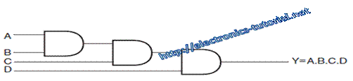
Figure above shows the four-input AND gate using two-input AND gates.
1) The first AND produces the output1=A.B.
2) The second AND gate produces the output2 = output1. C.
3) The third AND gate produces the output3 = output2. D.
4) Therefore, finally Y= A.B.C.D
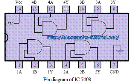
TTL AND gate ICs
1) 7408 Quad two-input AND gate
2) 7409 Quad two-input AND gate (open collector)
3) 7411 Triple three-input AND gate
4) 7421 Dual four-input AND gate
CMOS AND gate ICs
1) 4081B Quad two-input AND gate
2) 4073 Triple 3-input AND gate
3) 4082 Dual 4-input AND gate
ECL AND gate ICs
1) 10104 Quad two-input AND gate