Home > mini projects > THREE STAGE AMPLIFIER WITH CURRENT LIMITER
THREE STAGE AMPLIFIER WITH CURRENT LIMITER
Abstract - The performance obtainable from a single-stage amplifier is often insufficient for many applications, so several stages may be combined forming a multistage amplifier. These stages are connected in cascade, i.e. output of the first stage is connected to form input of second stage, whose output becomes input of third stage, and so on. The overall gain of a multistage amplifier is the product of the gains of the individual stages . The three stage amplifier with current limiter consists of three stages namely Differential Amplifier , Combination of diodes and resistor circuit and the current limiter
. A differential amplifier is a type of electronic amplifier that amplifies the difference between two input voltages but suppresses any voltage common to the two inputs. Current limiting is the practice of imposing an upper limit on the current delivered to a load with the purpose of protecting the circuit from short-circuit replaced by Multi-stage transistor amplifiers.In Multi-stage amplifiers, the output of first stage is coupled to the input of next stage using a coupling device. These amplifiers receive audio signals from the audio source, amplify those signals, generate audio current signals based on those amplified signals, and output the current signals to the speakers. It is these current signals that drive the speakers and cause them to reproduce the audio signals that are generated by the audio source to create sound. In three stage amplifier the first stage consists of a differential amplifier,second stage consists of a coupling device as a combination of diodes and third stage uses a current limiter. The three stages are: First stage-Differential amplifier, Second stage-Combination of diodes, Third stage-Current limiter
I. INTRODUCTION
Here we have implemented a three-stage amplifier, which will amplify an audio signal from a headphone jack and drive a low-impedance speaker or used in any other device which require the amplification of input signal. Multistage amplifiers are urgently needed with the advance in technologies, due to the fact that single-stage cascode amplifier is no longer suitable in low-voltage designs. Moreover, short-channel effect of the sub-micron CMOS transistor causes output-impedance degradation and hence gain of an amplifier is reduced dramatically.
In practical applications, the output of a single stage amplifier is usually insufficient, though it is a voltage or power amplifier. Hence they are
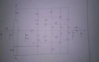
Figure.1
I. First stage
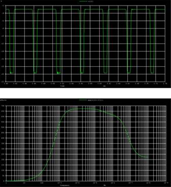
The first stage consists of differential amplifier. This differential amplifier is used in dual input, balanced output configuration. As the sinusoidal input is given at the base terminal of one of the transistors and the second input is obtained from the second stage. The output is taken at the collectors of both the transistors which are at same dc potential with respect to ground. Thus is differential amplifier works in dual input,balanced output configuration.
Two matched semiconductor transistors of the same type (BJTs) are required for the differential amplifier. All the components of the two - emitter biased transistors circuits, which constitute a differential amplifier, must be matched in all respect for proper operation.
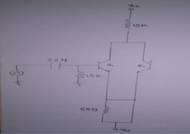
Figure 2
Also the magnitude of supply voltages +Vcc and -Vee must be equal. Here, in three stage amplifier we have used the magnitude as (Vcc=10V and Vee= -10V) . A multistage amplifier can be obtained by direct connection between successive stages of differential amplifier. The direct connection between stages removes lower cut-off frequency imposed by the coupling capacitors. But in direct connection between successive stages the gain obtained is not appreciable or not upto that extent which is required at the output terminal. So we have used here the middle stage that is the second stage wherein resistors and diodes are connected so that the transistors are biased.
The input is given a sine wave with 10V peak to peak.The input is given at the base of one of the transistors and the second input to the transistor is fed from the second stage. The output is taken from the collector of the two transistors. The two transistors used are npn transistors.
Thus this differential amplifier thus amplifies the difference between the input signals applied at the two input terminals.
OBSERVATIONS for stage 1:
The output is observed at the collector of two transistors. The output is the amplified signal of the difference between the two input terminals.
Vout = Ad(V2-V1)
This amplified output is given to next stage for further amplification. The next stage amplification is done bya network which is a combination of diodes and resistors.
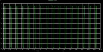
SIMULATION RESULT:
FIRST STAGE:
II. SECOND STAGE
The second stage amplification is done by a network which is made up of combination of resistors and diodes.
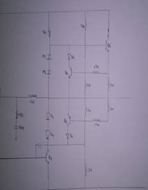
Figure 3
The middle stage primarily serves as an AC and DC buffer between the two stages. If we were to directly cascade the input and output stages together, the following two things would happen:
1. Because the bias current of the output stage is so much higher than the input stage, the base of the output drive transistor would draw significant current from resistor and and totally alter the output bias point of the input stage.
2. The output impedance of the input stage and the input impedance of the output stage are of similar magnitudes. Not all of the voltage generated by the input stage would be coupled to the output stage due to the loading effect.
This stage even uses a single slope circuit protection.
SIMULATION RESULT:
SECOND STAGE:
3
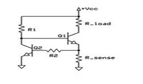
Figure 3
The above figure of current limiter operate more efficiently from a single (Vcc) supply. R1 allows Q1 to turn on and pass voltage and current to the load. When the current through R_sense exceeds the design limit, Q2 begins to turn on, which in turn begins to turn off Q1, thus limiting the load current. The optional component R2 protects Q2 in the event of a short-circuited load. WhenVcc is at least a few volts, a MOSFET can be used for Q1 for lower dropout voltage. Due to its simplicity, this circuit is sometimes used as a current source for high-power LEDs. But here we cannot use MOSFETs because Vcc used here is 25V.
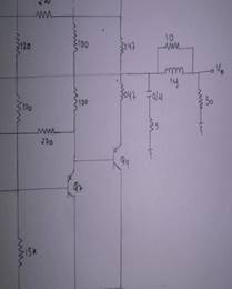
Figure 4
III. THIRD STAGE
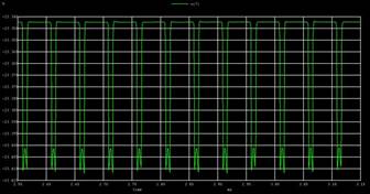
The third stage is the output stage.It includes a current limiter. Current limiting is the practice in electrical orelectronic circuits of imposing an upper limit on the current that may be delivered to a load with the purpose of protecting the circuit generating or transmitting the current from harmful effects due to a short-circuit or similar problem in the load.
The parallel combianation of resistor and inductor and also a capacitor in series with it provides slow edge rate which improves electromagnetic compatibility.
The output obtained is amplified input signal which could be used to give to an audio amplifier and to other devices which require voltage amplification.
SIMULATION RESULT:
OUTPUT STAGE: