To achieve optimum performance in a digital system, devices from more than one logic family can be used, taking advantages of the superior characteristics of each family for different parts of the system. For example, CMOS logic ICs can be used in those parts of the system where low power dissipation is required, whereas TTL can be used for those portions of the system which require high speed of operation. Also, some function may be easily available in TTL and others may be available in CMOS. Therefore, it is necessary to examine the interface between CMOS and TTL devices.
CMOS and TTL are the two most widely used logic families. Although ICs belonging to the same logic family have no special interface requirements, that is, the output of one can directly feed the input of the other, the same is not true if we have to interconnect digital ICs belonging to different logic families. Incompatibility of ICs belonging to different families mainly arises from different voltage levels and current requirements associated with LOW and HIGH logic states at the inputs and outputs.
CMOS driving TTL:
Following figure shows a CMOS gate driving N TTL gates. For such an arrangement to operate properly the following conditions are required to be satisfied,
VOH (CMOS) ≥ VIH(TTL)
VOL (CMOS) ≤ VIL(TTL)
– IOH (CMOS) ≥ NIIH(TTL)
IOL (CMOS) ≥ – NIIL(TTL)
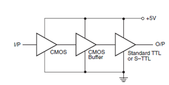
The first possible type of CMOS-to-TTL interface is the one where both ICs are operated from a common supply. We have read in earlier sections that the TTL family has a recommended supply voltage of 5 V, whereas the CMOS family devices can operate over a wide supply voltage range of 3–18 V. In the present case, both ICs would operate from 5 V. As far as the voltage levels in the two logic states are concerned, the two have become compatible. The CMOS output has a VOH(min.) of 4.95V (for VCC =5 V) and a VOL(max.) of 0.05 V, which is compatible with VIH(min.) and VIL(max.) requirements of approximately 2 and 0.8V respectively for TTL family devices. In fact, in a CMOS-to- TTL interface, with the two devices operating on the same VCC, voltage level compatibility is always there. It is the current level compatibility that needs attention. That is, in the LOW state, the output current-sinking capability of the CMOS IC in question must at least equal the input current-sinking requirement of the TTL IC being driven. Similarly, in the HIGH state, the HIGH output current drive capability of the CMOS IC must equal or exceed the HIGH-level input current requirement of TTL IC. For a proper interface, both the above conditions must be met. As a rule of thumb, a CMOS IC belonging to the 4000B family (the most widely used CMOS family) can feed one LS TTL or two low-power TTL unit loads. When a CMOS IC needs to drive a standard TTL or a Schottky TTL device, a CMOS buffer (4049B or 4050B) is used. 4049B and 4050B are hex buffers of inverting and noninverting types respectively, with each buffer capable of driving two standard TTL loads.
Figure below shows a CMOS-to-TTL interface with both devices operating from 5V supply and the CMOS IC driving a low-power TTL or a low-power Schottky TTL device.
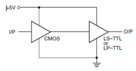
Figure below shows a CMOS-to-TTL interface where the TTL device in use is either a standard TTL or a Schottky TTL.
The CMOS-to-TTL interface when the two are operating on different power supply voltages can be achieved in several ways. One such scheme is shown below. In this case, there is both a voltage level as well as a current level compatibility problem.

TTL Driving CMOS :
For TTL gate driving N CMOS gates arrangement to operate properly, the following conditions are required to be satisfied:
VOH (TTL) ≥ VIH(CMOS)
VOL (TTL) ≤ VIL(CMOS)
– IOH (TTL) ≥ NIIH(CMOS)
IOL (TTL) ≥ – NIIL(CMOS)
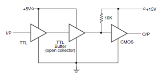
In the TTL-to-CMOS interface, current compatibility is always there. The voltage level compatibility in the two states is a problem. VOH (min.) of TTL devices is too low as regards the VIH (min.) requirement of CMOS devices. When the two devices are operating on the same power supply voltage, that is, 5 V, a pull-up resistor of 10 k_ achieves compatibility as shown in below figure.
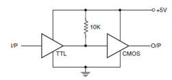
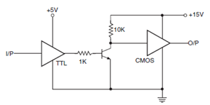
The pull-up resistor causes the TTL output to rise to about 5V when HIGH. When the two are operating on different power supplies, one of the simplest interface techniques is to use a transistor (as a switch) in-between the two, as shown below.
Another technique is to use an open collector type TTL buffer as shown below.
CMOS QUIZ:
CMOS Family