Successive Approximation type ADC is the most widely used and popular ADC method. The conversion time is maintained constant in successive approximation type ADC, and is proportional to the number of bits in the digitaloutput, unlike the counter and continuous type A/D converters. The basic principle of this type of A/D converter is that the unknown analog input voltage is approximated against an n-bit digital value by trying one bit at a time, beginning with the MSB. The principle of successive approximation process for a 4-bit conversion is explained here. This type of ADC operates by successively dividing the voltage range by half, as explained in the following steps.
(1) The MSB is initially set to 1 with the remaining three bits set as 000. The digital equivalent voltage is compared with the unknown analog input voltage.
(2) If the analog input voltage is higher than the digital equivalent voltage, the MSB is retained as 1 and the second MSB is set to 1. Otherwise, the MSB is set to 0 and the second MSB is set to 1. Comparison is made as given in step (1) to decide whether to retain or reset the second MSB.
The above steps are more accurately illustrated with the help of an example.
Let us assume that the 4-bit ADC is used and the analog input voltage is VA = 11 V. when the conversion starts, the MSB bit is set to 1.
Now VA = 11V > VD = 8V = [1000]2
Since the unknown analog input voltage VA is higher than the equivalent digital voltage VD, as discussed in step (2), the MSB is retained as 1 and the next MSB bit is set to 1 as follows
VD = 12V = [1100]2
Now VA = 11V < VD = 12V = [1100]2
Here now, the unknown analog input voltage VA is lower than the equivalent digital voltage VD. As discussed in step (2), the second MSB is set to 0 and next MSB set to 1 as
VD = 10V = [1010]2
Now again VA = 11V > VD = 10V = [1010]2
Again as discussed in step (2) VA>VD, hence the third MSB is retained to 1 and the last bit is set to 1. The new code word is
VD = 11V = [1011]2
Now finally VA = VD , and the conversion stops.
The functional block diagram of successive approximation type of ADC is shown below.
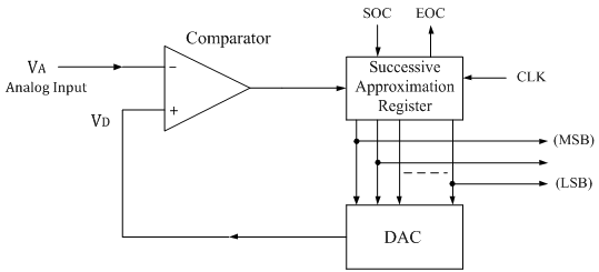
It consists of a successive approximation register (SAR), DAC and comparator. The output of SAR is given to n-bit DAC. The equivalent analog output voltage of DAC, VD is applied to the non-inverting input of the comparator. The second input to the comparator is the unknown analog input voltage VA. The output of the comparator is used to activate the successive approximation logic of SAR.
When the start command is applied, the SAR sets the MSB to logic 1 and other bits are made logic 0, so that the trial code becomes 1000.
Advantages:
1 Conversion time is very small.
2 Conversion time is constant and independent of the amplitude of the analog input signal VA.
Disadvantages:
1 Circuit is complex.
2 The conversion time is more compared to flash type ADC.