Home > Digital CMOS Design > Non Ideal Effects > Mobility Variation
Mobility Variation | Digital-CMOS-Design
Mobility Variation
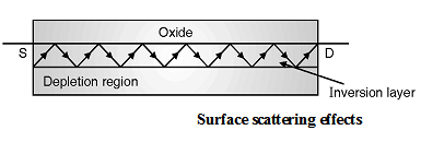
In the derivation of ideal I-V relationship we assumed that the mobility was constant. This assumption must be modified for two reasons. The first reason is the variation of mobility with gate voltage and the second reason is that the effective carrier mobility decreases as the carrier approaches the velocity saturation limit as discussed previously. The inversion layer is created by a vertical electric field because of gate voltage. A positive gate voltage produces a force on the electrons in the inversion layer towards the surface. As the electrons travel through the channel towards the drain they are attracted to the surface but then are repelled by localized coulombic forces. This effect is shown in
Figure and called as surface scattering.
The effective carrier mobility is only a function of the electric field at the inversion layer and is independent of oxide thickness. The effective mobility is given by,
eff = 0 EeffE0 1/3
Where 0 and E0 are constants determined from experimental results.
The effective inversion charge mobility is strong function at temperature because of lattice scattering. As the temperature is reduced the mobility increases.