The Phase Locked Loop concept was first developed in 1930. Since then it is used in communication systems of different types, particularly in satellite communication system. Before the invention of IC PLL, systems were very complex and costly for use in most consumer & industrial systems. Now PLL ICs are fabricated at a very low cost. Therefore their use has become attractive for many applications such as FM demodulator, Stereo demodulators, Tone detectors, frequency synthesizers etc. Bellow figure shows the block diagram of PLL which consists of phase detector, LPF, error amplifier and Voltage controlled oscillator.
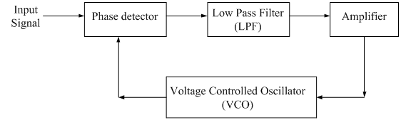
The phase detector block has two inputs, external signal and oscillator signal. Phase detector detects the phase between two signals and develops an output voltage proportional to phase difference. This block also called as phase detector or phase comparator. Output of phase detector is passed through a LPF. It removes high frequency signal and passes only low frequencies. This filter is also called as loop filter because the PLL system is a closed loop system. Output of filter is amplified by amplifier. This amplified output is applied as input for VCO. This input voltage adjusts the frequency of VCO such that the VCO frequency is equal to signal frequency i.e. VCO converts input voltage into frequency i.e. acts as voltage to frequency converter.
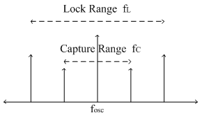
When the signal frequency and VCO frequency is same the loop gets locked. The loop gets locked by detecting the phase difference between two inputs so called Phase Locked Loop (PLL). Without application of any external signal, VCO has some frequency called as free running frequency or centre frequency. In this initial condition loop is not locked i.e. in open condition.
When external signal is applied its frequency is either less or greater than VCO frequency so there is a phase difference between them. Phase detector detects the phase difference between two inputs and generates an error voltage. This is passed through LPF. After amplification it is given as a controlled voltage. This adjusts the frequency of VCO such that input frequency is equal to VCO frequency and forms locked condition.This process of locking the loop is called Capture effect.
The time required for VCO to adjust its frequency with signal frequency is called capture time. It depends on the internal parameters of system. There is some limit for input signal for which system can acquire a locked condition. This range of frequency between which the system can goes into locked condition is called capture range. This range is symmetrical about centre frequency. This capture range depends upon filter and amplifier characteristics.
If system acquires a locked condition then even if the signal frequency changes the loop remains in locked condition. The range of input frequency over which the locked condition maintained is called locked range. This also depends on amplifier and filter characteristics. Capture range is always less than lock range or almost equal; but capture range is never greater than locked range.
The following figure shows the PLL spectrum of the three frequencies.
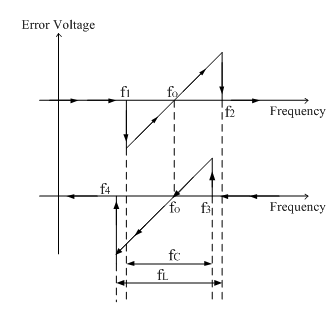
Let Input signal is , Vin=Vs sinωs VCO ouput signal is , Vout=Vo sin(ωot+ɸ) Phase detector is a non-linear device. Therefore the output of phase detector is proportional to the product of two inputs. In practice, the two input frequencies for phase detector block are not same and hence the error voltage is generated. Transfer characteristics of PLL:
Initially the signal frequency is gradually increased. The PLL is not locked because signal frequency and VCO frequency is not same. At frequency f1, the PLL is locked. Thus f1 is referred as lower edge of the capture range. After f1 PLL remains in locking condition. At frequency f1a sudden negative jump of error voltage is observed to shift the output frequency fo of VCO. If signal frequency is still increased, the loop remains in locked condition. At frequency f2 the locked condition is lost. So frequency f2 is called as upper edge of the lock range. After f2, lock is removed and error voltage drops to zero and VCO frequency returns to its free running frequency. If the signal frequency is gradually decreased, the loop is captured at frequency f3 and removed at frequency f4 (i.e. between f3 and f4 the locking condition is maintained). Thus f3 is called as upper edge of the capture range and f4 is called as upper edge of lock range. Thus frequency range between f3 and f1 is called capture range and frequency range between f4 and f2 is called lock range. Capture range. The typical voltage to frequency transfer characteristics of PLL are shown below,
Phase Detector/Comparator: Phase detector is an important part of PLL system. There are two types of phase detectors are used, analog and digital.
Analog phase detector:
The analog phase detector is basically a simple electronic switch as shown in figure below,
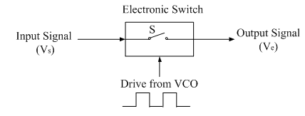
The principle of analog phase detection using switch type phase detector is shown above. An electronic switch is opened and closed by signal coming from VCO (normally a square wave) as shown in figure. The input signal is therefore chopped at a repetition rate determined by VCO frequency. The following figure shows the input signal Vs assumed to be in phase (ɸ=0̊) with VCO output.

Since the switch is closed only when VCO output is positive, the output waveform (error voltage) Ve will be half sinusoids. Similarly, the output waveforms for ɸ = 90̊ and ɸ = 180̊ is shown in figure. This type of phase detector is called a half wave detector, since the phase information for only one-half of the input waveform is detected and averaged. The output of the phase comparator when filtered through a low pass filter gives an error signal which is the average value of the output waveform shown by dotted line in figure. It may be seen that the error voltage is zero when the phase shift between the two inputs is 90̊. So to achieve a perfect locked condition, the VCO output should be 90̊ out of phase with respect to the input signal.
Digital phase detector:
The following figure shows the digital type Ex-OR (Exclusive OR) phase detector. The output of the EX-OR gate is HIGH only when one of the input signals is high.
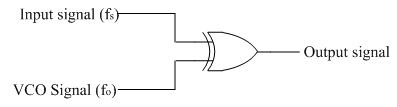
These types of phase detectors are used when both the inputs are square waves. The input and output waveforms are shown below.
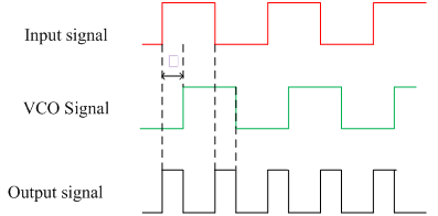
Here input signal leads VCO output by ɸ°.
The variation of dc output voltage with phase difference ɸ is shown in figure bellow,
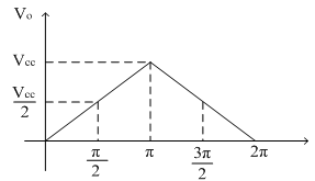
It can be seen that the maximum dc output voltage occurs when the phase difference is π (180̊) because output of the gate remains high throughout. The slope of the curve gives the conversation ratio kɸ of the phase detector. EX-OR phase detector can be realized using ICs such as CD 4070. The output dc voltage depends on the duty cycle of the input waveforms. Therefore, this type of phase detector is employed when the waveforms of input signal and output signal are square waves with 50% duty cycle.