Introduction to MOSFETS (Metal Oxide Semiconductor Field Effect Transistor)
The MOSFET transistor is a semiconductor device which is widely useful for switching and amplifying electronic signals into the electronic devices.
If you check below figure of Structure of NMOS transistor. Basically it shows the simplified structure associated with the NMOS transistor. The NMOS transistor is fabricated on a p type substrate called as 'bulk' or 'body'. The two heavily doped n+ regions are diffused in the p type substrate which forms the source and drain terminals. A heavily doped (conducting) piece of polysilicon which is in fact called as poly is operates as a gate terminal. A thin layer of silicon dioxide (SiO2) will act as insulating material between poly and substrate. A junction formed between SiO2, substrate and poly is called as MOS (metal-oxide-semiconductor) junction. The useful action i.e. formation of channel is occurred within the substrate region which is laying under the gate oxide. The dwelling is symmetric with regards to drain and source.
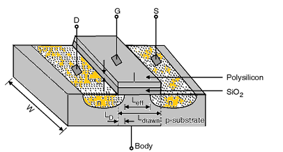
The dimension regarding the gate along the source drain path is called once the length 'L' plus the dimension perpendicular to your length is called as width 'W' associated with the transistor. The ratio of width to length is called as 'W'/L ratio which plays important role in digital designs.
Throughout the fabrication of Source and Drain junction the dopants are “side diffuse†this is why the actual distance between source and drain is slightly lower than 'L'.
Therefore Leff = Ldrawn – 2LD where Leff works well length, Ldrawn is the total LD and length is the amount of side diffusion. The thickness of oxide tox is the important parameter which decides the oxide capacitance Cox. The principle thrust in MOS technology development is to reduce both Leff and tox from a single generation to another without degrading other device parameters.
MOSFET SWITCH
The metal-oxide-semiconductor field effect transistor (MOSFET) is the important semiconductor device for digital and analog integrated circuit designs. Its major asset from digital perspective is that it performs very well as a switch and it introduces very few parasitic effects. Other important advantages are its integration density combined with a relatively simple manufacturing process, which make it possible to produce large and complex circuits in an economical way. The MOSFET is a four terminal device. The voltage applied to the gate terminal controls the current flow between the source and drain parts. The body represents the fourth terminal of the transistor. Its function is secondary because it only serves to modulate the device characteristics and parameters.
For digital circuit design the transistor is thought as a switch. When the voltage is applied to the gate which is larger than the threshold voltage (VT) a conducting channel is formed between drain and source. In the presence of voltage difference between source and drain electrical current flows from drain to source. The conductivity of the channel is modulated by the gate voltage. If the voltage difference between gate and source is large then the resistance of the conducting channel is small and larger current flows through the channel. When the gate voltage is lower than the threshold no such channel exists and the switch is considered as open.
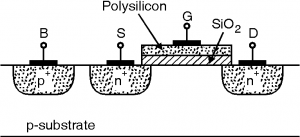
Fig .1
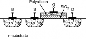
Fig. 2
Two types of MOSFET devices can be identified. The N channel MOSFET shortly NMOS and P channel MOSFET shortly PMOS. The NMOS transistor consists of n+ drain and source regions embedded in a p-type substrate as shown in Fig 1. The current is carried by electrons moving through an n-type channel between source and drain. This is in contrast to the pn junction diode where current is carried by both holes and electrons. In PMOS devices an p+ drain and source regions are embedded in a n-type substrate as shown in Fig. 2. In such a transistor current is carried by holes moving through a p type channel formed below the SiO2 layer. In a complementary MOS (CMOS) technology both devices are present. The cross section of n-well CMOS process is shown in Fig. 3.
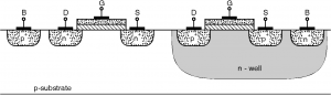
Fig.3
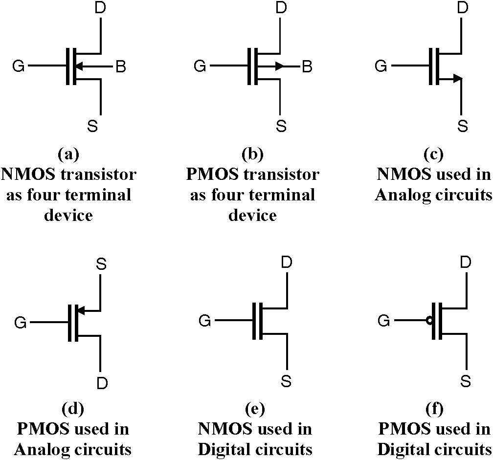
Circuit symbols for the various MOS transistors are shown in Fig. 4. As mentioned earlier the transistor is a four port device with gate, source, drain and body terminals (Fig. 4 (a) and (b)). Since the body is generally connected to a DC supply i.e. Ground for NMOS and VDD for PMOS. Most of the time body is not shown on the schematics (Fig. 4 (c), (d), (e) and (f)). If the fourth terminal is not shown in the schematic then it is assumed that the body is connected to the appropriate supply.