Home > mini projects > 3 BIT PARALLEL to SERIAL DATA CONVERTER
DATA CONVERTER
Abstract - This report enumerates the analysis and design of a circuit containing D-Flip Flops to form 3 - Bit Parallel Input Serial Output Shift Register using NGSPICE software. The main objective is to convert 3- bit parallel input data into serial output data. The flip flop is used to store data and for shifting purpose. Design and simulation of the convertor has been carried out using NGSPICE software.
I. INTRODUCTION
A register is a group of flip-flops that is required to store binary information. Parallel Input Serial Output Shift Register is a type of sequential logic circuit, mainly for conversion of data. They are group of edge-triggered D-Flip Flop cascaded one after another. All the Flip Flops are driven by same clock input & all are set or reset simultaneously. Parallel data is loaded into register simultaneously
& is shifted out serially one bit at a time under clock control.
II. NEED OF PARALLEL IN SERIAL OUT SHIFT REGISTER
In communication, Parallel Communication requires a lot of hardware and hence the cost of the system goes on increasing. Therefore, Serial Communication is used, as the hardware requirement is reduced. In communication, transmitter uses parallel in serial out shift register to convert parallel data in serial form for communication between different systems.This reduces the number of parallel connections required in the circuit and hence reducing the hardware cost.
In microprocessor, data is read into it using parallel in serial out. It is good for gathering a large number of inputs, like buttons.
III. WORKING
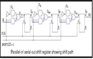
The input data is connected individually to each D-flip flop through mux & the clock input is directly connected to all flip flops. Here DA, DB, DC are simultaneously given to shift register. Shift/load' (SH/LD') is connected to all multiplexers. When SH/LD' is low & negative edge triggered clock pulse is given to flip flop, the data is loaded in all D-flip flops. When SH/LD' is high & negative edge triggered clock pulse is given to flip flop, the data in flip flops is serially shifted out by one bit. Then after every negative edge pulse, data is shifted bit by bit. After shifting all 3 bits, new data is loaded into the shift register.
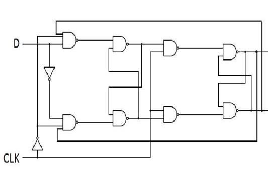
IV. CIRCUIT
D - Flip flop
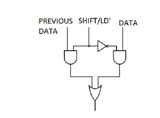
Mux using gates
VI. TIMING DIAGRAM
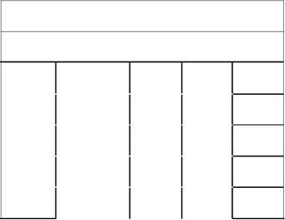
For the parallel data input
Assume DA=1, DB=0, DC=1
|
Clock |
Shift/Load' |
Q0 |
Q1 |
Q2 |
|||
|
1 |
|||||||
|
1 |
Load |
1 |
0 |
||||
|
0 |
|||||||
|
2 |
Shift |
0 |
1 |
||||
|
1 |
|||||||
|
3 |
Shift |
0 |
0 |
||||
|
0 |
|||||||
|
4 |
Load |
0 |
0 |
||||
VII. COMPONENTS
A. Components :
1. D-flip flops (x3): D-flip flops are cascaded to make a shift register.
2. AND Gate (x6): The output from AND gate is used to make multiplexer.
3. NAND Gate (x24): The NAND gate is used for making D- Flip Flop. Three input and two input NAND gates are used.
4. OR Gate (x3) : The output from OR gate is used to make multiplexer.
5. Inverter (x3): Inverter gate is used for Shift/Load' and various other inputs.
B. Clock Inputs:
Different Clock inputs are required for the working of circuit depending on the rate of
transmission. Clock is also used to govern control signals.
Input Waveforms :
» Data A
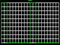
» Data B
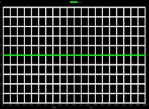
» Data C
» Clock
» Shift/Load'
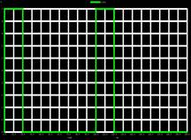
Output Waveforms :
» Serial Output Data