Home > Digital CMOS Design > CMOS Layout Design > CMOS lambda Design Rules
CMOS lambda Design Rules
CMOS 'λ' Design Rules :
The MOSIS stands for MOS Implementation Service is the IC fabrication service available to universities for layout, simulation, and test the completed designs. The MOSIS rules are scalable λ rules.
The MOSIS design rules are as follows :
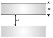
(1) Rules for N-well as shown in Figure below.
1. Minimum width = 10λ
2. Wells at same potential with spacing = 6λ
3. Wells at same potential = 0λ
4. Wells of different type, spacing = 8λ
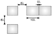
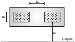
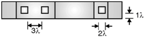
(2) Rules for Active area shown in Figure below.
1. Minimum width = 3λ
2. Minimum spacing = 3λ
3. Source/Drain active to well
edge = 5λ
4. Substrate/well contact active
to well edge = 3λ
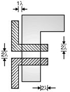
3) Rules for poly 1 as shown in Figure below.
1. Minimum width = 2λ
2. Minimum spacing = 2λ
3. Minimum gate extension of active = 2λ
4. Minimum field poly to active = 1λ
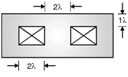
(4) Rules for contact to poly 1 as shown in Figure below.
1. Exact contact size = 2 λ 2 λ
2. Minimum poly 1 overlap = 1 λ
3. Minimum contact spacing = 2 λ
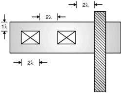
(5) Rules for contact to active as shown in Figure below. 1. Exact contact size = 2λ 2λ 2. Minimum active overlap = 1λ 3. Minimum contact spacing = 2λ 4. Minimum spacing to gate of transistor = 2λ
(6) Rules for metal 1 as shown in Figure below.
1. Minimum width = 3λ
2. Minimum spacing = 3λ
3. Minimum overlap of poly contact = 1λ
4. Minimum overlap of active contact = 1λ
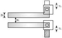
(7) Rules for via 1 as shown in Figure below.
1. Minimum size = 2λ λ
2. Minimum spacing = 3λ
3. Minimum overlap by metal 1 = 1λ
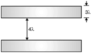
(8) Rules for metal 2 as shown in Figure below.
1. Minimum size = 3λ
2. Minimum spacing = 4λ
(9) Rules for metal 3 as shown in Figure below.
1. Minimum width = 6λ
2. Minimum spacing = 4λ