Boundary Scan Standards :
To better address problems of board-level testing, several design for testability standards have been developed. The primary goal of these proposed standards is to ensure that chips of VLSI complexity contain a common denominator of DFT circuitry that will make the test development and testing of boards containing these chips significantly more effective and less costly. Some of these initiatives are known as the Joint Test Action Group (JTAG).
- No need for complex testers in PCB testing.
- The test engineer’s work is simplified and efficient.
- The time spent on test pattern generation and application is reduced.
- Fault coverage is increased.
Boundary Scan 1149.1 Standard :
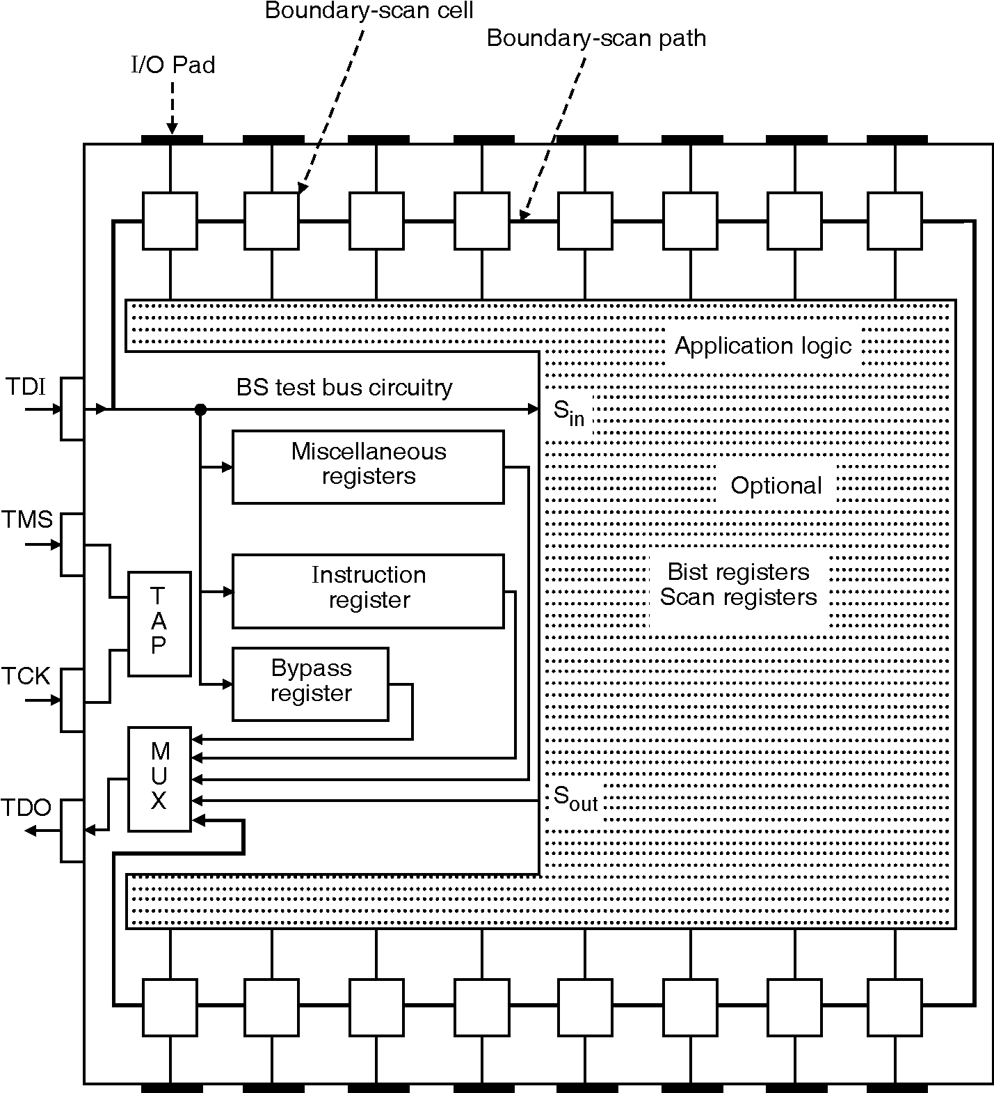
The standards discussed above deal primarily with the use of a test bus which will reside on a board, the protocol associated with this bus, elements of a bus master which controls the bus, I/O ports that tie a chip to the bus, and some control logic that must reside on a chip to interface the test bus ports to the DFT hardware residing on the application portion of the chip. In addition, the JTAG boundary scan and IEEE 1149.1 standards also require that a boundary-scan register exist on the chip. The description of a board-level test bus presented on IEEE 1149.1. Figure below shows a general form of a chip which supports IEEE 1149.1. The application logic represents the normal chip design prior to the inclusion of logic required to support IEEE 1149.1. The normal I/O terminals of the application logic are connected through boundary-scan cells to the chips I/O pads.The test-bus circuitry, also referred to as the bus slave consists of the boundary-scan registers, a 1-bit bypass register, an instruction register, several miscellaneous registers, and the TAP. The boundary-scan bus consists of four lines, that are a test clock (TCK), a test mode signal (TMS), the TDI line, and the TDO line. Test instructions and test data are sent to a chip over the TDI line. Test results and status information are sent from a chip over the TDO line serially. The sequence of operations are controlled by a bus master, which can be either ATE or a component that interfaces to a higher-level test bus Control of the test-bus circuitry is primarily carried out by the TAP, which responds to the state transitions on the TMS line.