Home > mini projects > Decoder and its Analysis
Decoder and its Analysis
Abstract - We review the main advantages in developing CMOS Decoder circuit. In addition to we describe its working principle. It can explain the advantages of basic Decoder and the thresholds of vatious parameters of circuit .Computer simulations show that the circuit has desirable desirable transfer characteristics than ones with resistors.We also compared our basic decoder circuit with the standard SN74LVC1G139 2-to-4 Line Decoder
I. Introduction
Ideally the Decoder circuit was made to decode the encoded information and here as its name indicates, a decoder is a circuit component that decodes an input code. Given a binary code of n-bits, a decoder will tell which code is this out of the 2^n possible codes. Thus, a decoder has n-inputs and 2^n outputs. Each of the 2^n outputs corresponds to one of the possible 2^n input combinations. Thus, each output line equals 1 at only one input combination but is equal to 0 at all other combinations.Now considering a 2 to4 decoder which is a building block to design any input decoder block more than two input whose output of the decoder is actually a minterm resulting from a certain combination of the inputs, that is
D0 =A1' A0', ( minterm m0) which corresponds to input 00
D1 =A1' A0, ( minterm m1) which corresponds to input 01
D2 =A1 A0', ( minterm m2) which corresponds to input 10
D3 =A1 A0, ( minterm m3) which corresponds to input 11
Applications:
Decoder applications many in the field of electonics and communication.Some of them are as follow
constuction of n Bit Decoder
NAND gate, Full Adder
BCD to decimal decoder
BCD to 7 segment decoder
Microprocessor memory systems
- Selecting different banks of memory
Microprocessor input/output systems
- Selecting different devices
Microprocessor instruction decoding
- Enabling different functional unit
Memory chips
- Enabling different row of memory depending on address
Solving the boolean expressions by additional gates
Specifications:
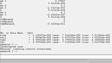
For the correct working of any any device specifications should be of great concern ,we cannot just despice them.Based on the model in Ngspice metal oxide semiconductors the circuit has good outputs when the voltage range from 4.0 v to 5v for logic 1 and 0v to 1v for logic 0 and input voltage VCC can be from 4.3v to 6.3v
Netlist for the simulation of decoder circuit:
Code:
.subckt inverter 1 3 0 2
.model MOSFETN nmos
m1 2 1 0 0 MOSFETN
.model MOSFETP pmos
m2 2 1 3 3 MOSFETP
.ends inverter
Code:
.model MOSFETN nmos
m1 4 1 3 0 MOSFETN
m2 3 2 0 0 MOSFETN
m5 6 4 0 0 MOSFETN
.model MOSFETP pmos
m3 4 1 5 5 MOSFETP
m4 4 2 5 5 MOSFETP
m6 6 4 5 5 MOSFETP
.ends AND
Code:
*2-i/p DECODER
x1 1 5 0 3 inverter
x2 2 5 0 4 inverter
.include and.cir
x3 3 4 5 0 7 and
x4 3 2 5 0 8 and
x5 1 4 5 0 6 and
x6 1 2 5 0 9 and
vdd 5 0 dc 5
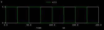
v1 1 0 pulse(0 5 0 0 0 25u 50u)
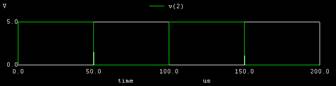
v2 2 0 pulse(0 5 0 0 0 50u 100u)
.tran 0.1u 200u
.control
run
display
Plot v(1)
Plot v(2)
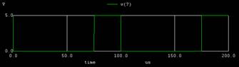
plot v(7)
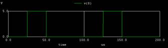
plot v(8)
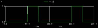
plot v(6)
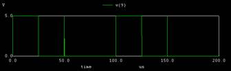
plot v(9)
.endc
.end
Explanation:
In the netlist given as in the figure below we used one subcicuit to generate a simulated inverter using CMOS in Ngspice and another subcircuit for generation of a AND circuit and the connections made to obtain the outputs.
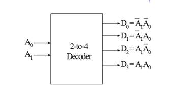
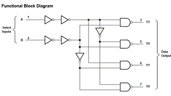
Let us discuss the operation and combinational circuit design of a decoder by taking the specific example of a 2-to-4 decoder. It contains two inputs denoted by A1 and A0 and four outputs denoted by D0, D1, D2, and D3 as shown in figure 2. Also note that A1 is the MSB while A0 is the LSB.
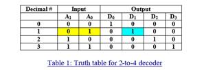
As we see in the truth table (table 1), for each input combination, one output line is activated, that is, the output line corresponding to the input combination becomes 1, while other lines remain inactive. For example, an input of 00 at the input will activate line D0. 01 at the input will activate line D1, and so on.
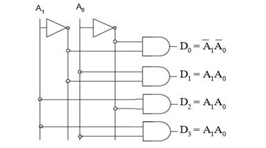
The circuit is implemented with AND gates, as shown in figure 3. In this circuit we see that the logic equation for D 0 is A1/ A0/. D0 is A1/ A0, and so on. These are in fact the minterms being implemented. Thus, each output of the decoder generates a minterm corresponding to the input combination.
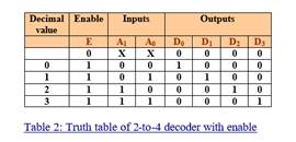
the enable input in decoder:
Generally, decoders have the "enable" input .The enable input perroms no logical operation, but is only responsible for making the decoder ACTIVE or INACTIVE.
* If the enable "E"
- is zero, then all outputs are zero regardless of the input values.
-is one, then the decoder performs its normal operation.
For example, consider the 2-to-4 decoder with the enable input (Figure 4). The enable input is only responsible for making the decoder active or inactive. If Enable E is zero, then all outputs of the decoder will be zeros, regardless of the values of A 1 and A 0. However, if E is 1, then the decoder will perform its normal operation, as is shown in the
truth table (table 2). In this table we see that as long as E is zero, the outputs D0 to D3 will remain zero, no matter whatever value you provide at the inputs A1 A0, depicted by two don't cares. When E becomes 1, then we see the same behavior as we saw in the case of 2-to-4 decoder discussedearlier.
Output waveforms
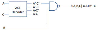
COMPARISION OF DECODER WITH standard SN74LVC1G139 2-to-4 Line Decoder
of SN74LVC1G139 2-to-4 Line Decoder
DC ANAYSIS:
vdd 5 0 dc 5
v1 1 0 dc 5
v2 2 0 dc 5
.dc v1 0 5 01
.dc v2 0 5 01
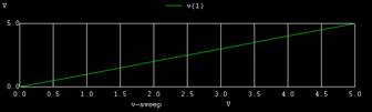
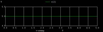
OUTPUTS:
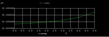
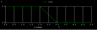
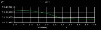
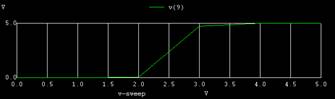
whose inputs are
this shows the theshold for 11 logic output at node 9 is high from the voltage 4.0 v similarly we can observe the thresholds for others output nodes.Here the standard version is providing a good range for logic 1.
When we compare with the components they provided the cicuit with extra two not gates which results in increment of chip size and the time delay for the output.
Time delay vs VCC for SN74LVC1G139 2-to-4 Line Decoder(TI):
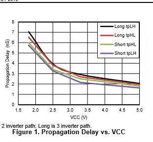
whereas the outputs for the tpd for one observation is found to
be 4.99ns which is 2ns less .