Home > Analog CMOS Design > MOSFET Parasitics > Source Drain Resistance
Source Drain Resistance
The shrinking technology and increasing frequencies are causing analog physical behavior in the device. The electrical parameters associated with final physical routes are called interconnected parasitics. The parasitic effects in the metal routes on the final silicon need to be estimated in the early phases of the design.
In the MOSFET structure, the typical parasitics are source-drain resistance, junction capacitance, overlap capacitance, gate resistance and interconnect RC components. However any parasitic resistances and capacitances that reduce the current drive or increase the node capacitance can also affect the MOSFET delay.
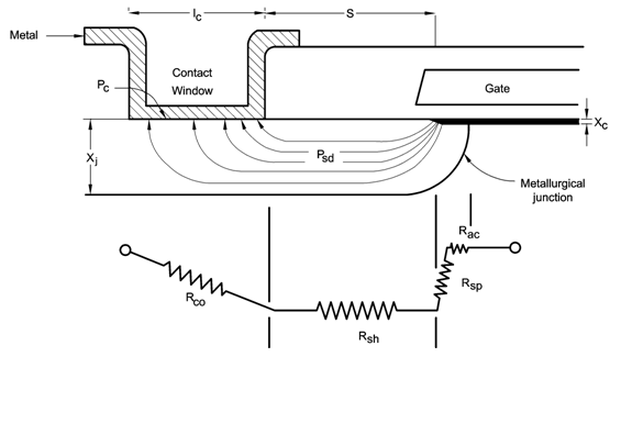
The Source-drain series resistance reduces the current of a short channel MOSFET.
The resistance on the source side is the most effective, since it reduces the gate drive voltage. Figure below shows the current flow pattern in the source or drain region of a MOSFET.
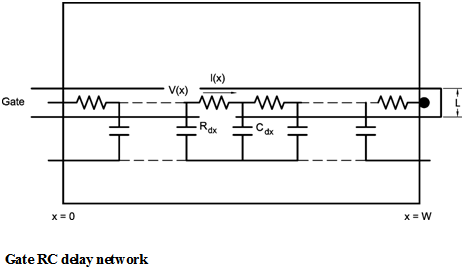
Gate Resistance :
The silicides are formed over polysilicon gates to lower the resistance and
provide ohmic contacts to both n+ and p+ gates. The
sheet resistivity of silicides is the order of
2-10 W/cm.
In combination with gate parasitic capacitances gate RC delay networks may form. Gate RC delay is an ac effect not observable in dc I-V curves. It shows up as an additional delay component in ring oscillators, delay chains and other logic circuits. The gate RC delay network is shown in Figure below.