Home > Digital CMOS Design > MOSFET Fundamentals > n channel Enhancement Mode MOSFET
n-channel Enhancement Mode MOSFET :
The cross-sectional view of n-channel enhancement mode MOSFET fabricated on p-type substrate is as shown in Figure. Further Figure shows the corresponding electrical symbol of the device.
As shown in Figure the NMOS is a four terminal device.
The substrate is universally Si. The insulator is Silicon dioxide (SiO2) and the gate material is poly-crystalline Si shortly called as poly Si. In Figure several important technological parameters of the device have been shown.
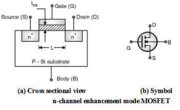
The lateral distances between the edges of the source and drain diffusions at the Si-SiO2 interface is known as the channel length (L). The depth of the device into the paper is known as the channel width (W) and the thickness of the oxide is given by tox. The substrate is assumed to be uniformly doped with the acceptor concentration of NA cm– 3. The basic idea behind the operation of n-channel enhancement MOSFET is to connect the majority carriers present in the drain and source diffusions which are electrons by a channel of carriers of the same type as the source and the drain (i.e. electrons) and opposite to that of the substrate (which are holes), that is why this channel is referred as the inversion channel. If a positive voltage is applied to the gate terminal it induces the electron inversion layer which connects the n type source and the n type drain regions.
Now, the existence of potential difference between source and drain ciuses the movement of electrons in the inversion channel and hence the drain current.