Home > mini projects > Serial To Parallel Convertor
Serial to Parallel Convertor
Abstract - In the actual scenario of communication, present day chips have parallel data bus but for long distance communication laying down parallel channels for every bit is costly and hardware consuming. Therefore, we use only a single channel to communicate between the two ports i.e. transmitter and receiver. For the receiver chips we use serial data from the channel and convert to parallel for future use.
I. INTRODUCTION
The task of a serial to parallel converter is to take a stream of data in serial format and for N-bit parallel converter, give N-bits as parallel output. Parallel data is required in several places like communication in a network, radar equipment etc. But the data cannot be fed to these systems in parallel format as the external hardware becomes cumbersome. A serial to parallel converter comes to rescue in these situations.
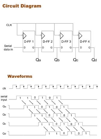
Serial to parallel convertor can also be considered as a serial-in parallel-out shift register. The basic structural component of the shift register is negative edge triggered D flip-flop. For N-bit serial to parallel convertor, N number of D flip-flops will be required.
Serial-in parallel-out can be converted to a serial-in serial-out by only considering the last stage.
II. NEED OF SERIAL TO PARALLEL CONVERTER
Parallel communication is essential in many systems. Parallel data thus is an inevitable part in many areas. But transmitting data in this format is not feasible in terms of hardware and cost
productivity. Here comes the need of serial to parallel converter. The transmitter section consists of a vice-versa parallel to serial converter and the receiver consists of serial to parallel converter.
A. Features
The converters can be a N-bit, implying the output can be obtained in N-bit parallel data. The clock frequency is 100kHz and the data rate is 10kHz. The data rate should be quite a factor less than clock frequency so as to obtain correct output waveforms.
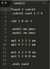
NAND gate using CMOS

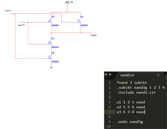
3-input NAND gate using 2-input NAND gate

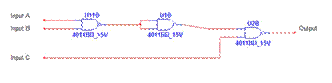
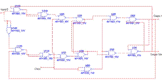
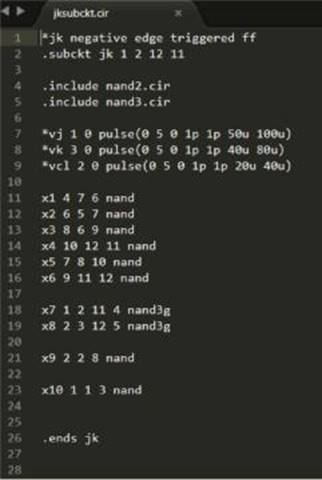
D-Flip flop using NAND gates

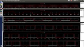
Simulation waveform
III. CONCLUSION
A 2-input NAND gate was simulated using CMOS technology
A 3-input NAND gate was simulated using 2-input NAND gate
A negative edge triggered D-flip flop was simulated using 2-input and 3-input NAND gates.
A serial to parallel converter was formed using 4 negative edge triggered D-flip flops.