Home > Analog CMOS Design > CMOS Differential Amplifier > Differential Amplifier
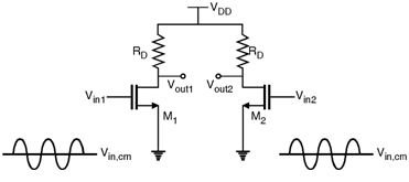
The important advantage of differential operation over single ended operation is higher immunity to noise. The simple differential amplifier is as shown in Figure below.
The other advantage of differential amplifier is the increase in voltage swings. The peak to peak swing differential amplifier is equal to 2 [V DD - (VGS - VTH)].
In the circuit of above Figure if Vin1 and Vin2 has a large common mode disturbances or unequal common mode dc level then the output response has distortions. As Vin, cm changes, bias currents of M1 and M2 also changes. Thus the transconductance of both the devices and output common mode dc level changes. The variation of the transconductance in turns leads to change in the small signal gain of the amplifier.
In order to solve the problem of common mode dc level the circuit shown in above figure is modified by employing a current source ISS to make (ID1 + ID2) independent of Vin, cm.
The modified circuit incorporating current source ISS is as shown in Figure below.
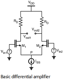
Thus, if Vin1 = Vin2 the biasing current of each transistor equals and the output common mode level is VDD - .
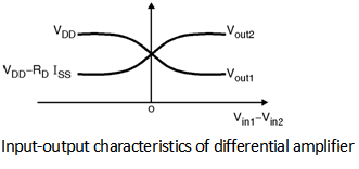
The input-output characteristics differential pair is as shown in Figure below.
In order to derive the voltage gain of the differential amplifier. Let us consider the circuit of basic differential amplifier
From Figure it is found that,
VGS1 = Vin1 - VP and VGS2 = V in2 - VP
\ Vin1 - VGS1 = Vin2 - VGS2
i.e. Vin1 - Vin2 = VGS1 - VGS2
Now, according to saturation current equation of MOSFET.
(VGS - VTH)2 =
\ VGS = + VTH
\ VGS1 = + VTH
and VGS2 = + VTH
Assuming equal dimensions of two transistors we get,
VGS1 - VGS2 = -
\ Vin1 - Vin2 = -
Take square on both sides.
(Vin1 - Vin2)2 = - +
(Vin1 - Vin2)2 = (ISS - 2 ) [ I D1 + ID2 = ISS]
i.e.
mn Cox (Vin1 - Vin2) 2 - ISS = - 2
Squaring on both sides,
(Vin1 - Vin2)4 - ISS mn Cox (Vin1 - Vin2)2 + ISS2 = 4 ID1 × I D2
But,
4 ID1 × ID2 = (ID1 + I D2)2 - (ID1 – ID2)2
= ISS2 - (ID1 - ID2) 2
By using this in the equation,
We get, (ID1 - ID2)2 = - (Vin1 - Vin2)4 + ISS mn C ox (Vin1 - Vin2)2
\ ID1 - ID2 = mn Cox (Vin1 - Vin2)
Thus, if Vin1 = Vin2 then ID1 - ID2 falls to zero, and increases from zero if | Vin1 - Vin2 | increases.
If ID1 - ID2 = D ID and V in1 - Vin2 = D Vin
\ = mn Cox
For D Vin = 0, The overall transconductance
Gm =
Hence, Vout1 - Vout2 = RD (ID1 - ID2)
= RD × Gm D Vin
\ = × RD
\ | An | = × RD
For a fully symmetric differential pair which senses inputs by equal and opposite amounts then the concept of half circuit can be applied to find the gain of the differential amplifier.
For the circuit shown in below Figure, by using the concept of half circuit, the small signal gain is given as,
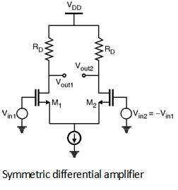
Vout1 = - gm (RD || ro) Vin1
Vout2 = - gm (RD || ro) (- Vin1 )
Vout1 - Vout2 = - gm (RD || ro) Vin1 - gm (RD || ro) Vin1
i.e. = - gm (RD || ro)
\ An = - gm (RD || ro)
Also, If Vin2 ¹ - Vin1 then using Half circuit concepts,
Vout1 = - gm (RD || ro) Vin1, V out2 = - gm (RD || ro) Vin2
Vout1 - Vout2 = - gm (RD || ro) (Vin1 - Vin2)
\ = - gm (RD || ro)
\ An = - gm (RD || ro)
Differential Pair with Current Source Loads :
In order to increase the gain of the amplifier the load resistance can be replaced by the current source load as shown in Figure below.
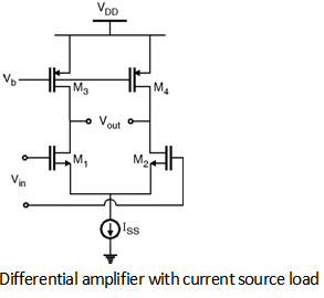
By using half circuit concept the gain can be given as :
An = - gm1, 2 (ro1, 2 || ro3, 4 )