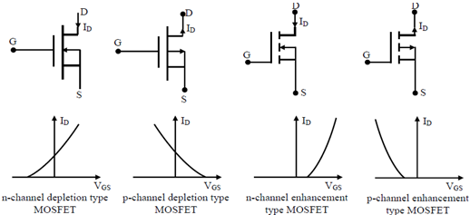
The power MOS field effect transistor (MOSFET) evolved from the MOS integrated circuit technology. Inherently fast switching speed of these devices can be effectively utilized to increase the switching frequency beyond several hundred kHz. MOSFET is controlled by the voltage applied on the control electrode (called gate) which is insulated by a thin metal oxide layer from the bulk semiconductor body. The electric field produced by the gate voltage modulates the conductivity of the semiconductor material in the region between the main current carrying terminals called the Drain (D) and the Source (S). Power MOSFETs, just like their integrated circuit counterpart, can be of two types (i) depletion type and (ii) enhancement type. Both of these can be either n- channel type or p-channel type depending on the nature of the bulk semiconductor. Figure below shows the various types of Power MOSFETs.
Constructional Features of a Power MOSFET:
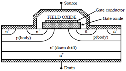
As mentioned in the introduction section, Power MOSFET is a device that evolved from MOS Integrated circuit technology. However it was soon realized that much larger breakdown voltage and current ratings could be achieved by resorting to a vertically oriented structure. A power MOSFET using VDMOS technology has vertically Oriented 3 layer structure of alternating p and n type semiconductors.
Operating principle of a MOSFET
When a small voltage is applied at the gate terminal positive with respect to the source (note that body and source are shorted) a depletion region forms at the interface between the SiO2 and the silicon. The positive charge induced on the gate metallization repels the majority hole carriers from the interface region between the gate oxide and the p type body. This exposes the negatively charged acceptors and a depletion region is created. Further increase in VGS causes the depletion layer to grow in thickness. At the same time the electric field at the oxide-silicon interface gets larger and begins to attract free electrons. The holes are repelled into the semiconductor bulk ahead of the depletion region. As VGS increases further the density of free electrons at the interface becomes equal to the free hole density in the bulk of the body region beyond the depletion layer. The layer of free electrons at the interface is called the inversion layer. The inversion layer has all the properties of an n type semiconductor and is a conductive path or “channel†between the drain and the source which permits flow of current between the drain and the source. Since current conduction in this device takes place through an n- type “channel†created by the electric field due to gate source voltage it is called “Enhancement type n-channel MOSFET. The value of VGS at which the inversion layer is considered to have formed is called the “Gate Source threshold voltage VGS (th)â€. As VGS is increased beyond VGS(th) the inversion layer gets somewhat thicker and more conductive, since the density of free electrons increases further with increase in VGS. The inversion layer screens the depletion layer adjacent to it from increasing VGS. The depletion layer thickness now remains constant. The MOSFET, like the BJT is a three terminal device where the voltage on the gate terminal controls the flow of current between the output terminals, Source and Drain.

Power MOSFET Operating modes
The source terminal is common between the input and the output of a MOSFET. The output characteristics of a MOSFET is then a plot of drain current (ID) as a function of the Drain –Source voltage (VDS) with gate source voltage (VGS). With Gate-source voltage (VGS) below the threshold voltage (VGS (th)) the MOSFET operates in the cut-off mode. No drain current flows in this mode and the applied drain–source voltage (VDS) is supported by the body-collector p-n junction. Therefore, the maximum applied voltage should be below the avalanche break down voltage of this junction (VDSS) to avoid destruction of the device. Consequently this mode of operation is called “ohmic mode†of operation. In power electronic applications a MOSFET is operated either in the cut off or in the ohmic mode. The slope of the VDS – ID characteristics in this mode is called the ON state Resistance of the MOSFET (RDS (ON)).
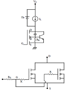
Gate Drive Circuitry of Power MOSFET
- MOSFET, being a voltage controlled device, does not require a continuous gate current to keep it in ON state. However, it is required to charge and discharge the gate-source and the gate- drain capacitors in each switching operation.
- The switching times of a MOSFET essentially depends on the charging and discharging rate of these capacitors. Therefore, if fast charging and discharging of a MOSFET is desired at fast switching frequency the gate drive power requirement may become significant.
- To turn the MOSFET on the logic level input to the inverting buffer is set to high state so that transistor Q3 turns off and Q1 turns on. Circuit during turn on. Note that, during turn On Q1 remains in the active region. Small resistances (R) are connected to individual gates before joining them together. This is because the gate inputs are highly capacitive with almost no losses. Some stray inductance of wiring may however be present.
- This stray inductance and the MOSFET capacitance can give rise to unwanted high frequency oscillation of the gate voltage that can result in puncture of the gate oxide layer due to voltage increase during oscillations. This is avoided by the damping resistance R.