Home > mini projects > Design of Astable Multivibrator Circuit
Design of Astable Multivibrator Circuit
Abstract:
The aim of this project is to design and implementation of astable multivibrator for many applications of communication systems.Here we used multivibrator circuit design by using different components like BJTs, resistors and capacitors. The circuit is simulated in NGSpice. An astable Multivibrator is constructed for given specification one of which is, it can vary its duty cycle from 10% to 90% and can have frequency range from 2 Hz to 100 KHz. Here we used the NGSpice simulation technique, which is very fast, and also bears the accuracy of circuit performance and reliability and the results are explored with browsing output data facility.
I. I NTRODUCTION
Astable multivibrator is a free running oscillator. It is a free running oscillator because it does not require any triggering. The first multivibrator circuit, the astable multivibrator oscillator, was invented by Henri Abraham and Eugene Bloch during World War I. The name multivibrator came into existence because the output contained many harmonics. Unlike the monostable multivibrator or the bistable multivibrator we looked at in the previous tutorials that require an "external" trigger pulse for their operation, the Astable Multivibrator has automatic built in triggering which switches it continuously between its two unstable states both set and reset. Astable multivibrator can have variable frequency and duty cycle. There are two types of astable multivibrator using BJT:
![]()
1) Emitter coupled astable multivibrator
2) Collector coupled astable multivibrator
The circuit that we are discussing is collector coupled astable multivibrator.
Advantages of collector coupled astable multivibrator over emitter coupled astable multivibrator:
1) The number of components required are less than emitter coupled astable multivibrator because emitter coupled astable multivibrator requires three supply voltages.
2) It is less costlier than collector coupled astable multivibrator.
3) In emitter coupled astable multivibrator switches between cutoff and active. This is a drawback as we need cutoff and saturation which is possible in collector coupled astable multivibrator.
II. L IST OF S YMBOLS USED
Q1, Q2 = Transistors
Vcc = Supply voltage
hfe = Common emitter current gain Output = Output voltage R3, R4 = emitter resistors
C1, C2 = coupling capacitors
III. C IRCUIT D IAGRAM
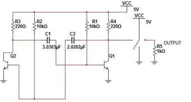
The Astable Multivibrator is another type of cross-coupled transistor switching circuit that has NO stable output states as it changes from one state to the other all the time. The astable circuit consists of two switching transistors, a cross-coupled feedback network, and two time delay capacitors which allows oscillation between the two states with no external triggering to produce the change in state.
The basic transistor circuit for an Astable Multivibrat or produces a square wave output from a pair of grounded emitter cross-coupled transistors. Both transistors either NPN or PNP, in the multivibrator are biased for linear operation and are operated as common emitter amplifiers with 100% positive feedback.
Let us assume that transistor Q1 is on and transistor Q2 is off. As transistor Q2 is off, the capacitor C1 charges through R3 till it reaches Vcc and as transistor Q1 is on, the capacitor C2 charges through R2 till it is less than 0.6V which is VBE(min).This makes the transistor Q2 to conduct and to move it into saturation region. As transistor Q2 moves into saturation region, it has a voltage drop Vce(sat)=0.2 across it. Before this capacitor C1 had Vcc-0.6v across it and as soon as transistor Q2 conducted, the capacitor plate connected to collector dropped to 0.2v.The other plate goes to -(Vcc-0.8) as capacitor does not allow sudden change in voltage. This will drive the transistor Q1 into cutoff region. This will lead to charging of C2 through R4 and C1 will charge till the negative end reaches more than 0.6v which will drive the transistor Q1 into conduction and then into saturation. This process goes on indefinitely and the output moves from voltage little lesser than Vcc and to voltage approximately 0.2v.In this specially we are using a wave shaping circuit in order to remove rise time problem which is implemented with the help of voltage controlled switch. When input voltage is high, the output is low and when input voltage is low, the output voltage is high.
V. D ESIGN C ONCEPTS
The period T = T1+T2
= 0.693 (R1xC1+R2xC2)
For symmetrical circuit with R1=R2=R and C1=C2=C T=1.38xRxC
We know that rise time, tr = 2.2 x Rc x C Hence,
![]()
Neglecting junction voltages, we get Ic=
![]() and Ib=
and Ib=
![]() To ensure saturation, Ib ≥
To ensure saturation, Ib ≥
R ≤ hfe x Rc and
By deciding hfe, we can decide the rising time to time period by 2 ratio.
Design of R and capacitor can be done accordingly from the table of resistors and capacitors.
Design of Rc:
![]() and
and
![]()
As we know hfe is variant accordingly by the above equation we can determine the value of Rc which is around R/hfe..
VI. S OME I MPORTANT P OINTS
1. Astable multivibrator has no stable states unlike monostable and bistable multivibrators which has got one and two stable states respectively. Therefore it switches between two states (in this case 0v and 5v).these states are generally known as quasi-stable states.
2. The amplitude of output waveform can be adjusted by varying the dc power supply. But it should not exceed 6v.
3. Output of astable multivibrator circuit is not a perfect square wave .to get a perfect square wave we need to add a wave shaping circuit after the astable multivibrator circuit.
4. The duty cycle can be adjusted by varying the values of capacitors accordingly.
5. The transistors used in these circuit acts as switches ie there are in saturation region. For a transistor to be in saturation region base-emitter junction and base-collector junction should be in forward bias condition.
|
Res. |
Capacitor values |
|||||||||
|
10nf |
22nf |
47nf |
100nf |
220nf |
470nf |
1000nf |
2200nf |
4700 |
||
|
1k |
72.15k |
32.8k |
15.35k |
7.215k |
3.28k |
1.535k |
721.5 |
328 |
153.5 |
|
|
2.2k |
32.79k |
14.9k |
6.98k |
3.28k |
1.49k |
698 |
328 |
149 |
69.8 |
|
|
4.7k |
15.35k |
6.97k |
3.26k |
1.53k |
697 |
326 |
153 |
69.7 |
32.6 |
|
|
10k |
7.215k |
3.28k |
1.535k |
721.5 |
328 |
153.5 |
72.15 |
32.8 |
15.35 |
|
|
22k |
3.28k |
1.49k |
698 |
328 |
149 |
69.8 |
32.8 |
14.9 |
6.98 |
|
|
47k |
1.535k |
697 |
326 |
153 |
69.7 |
32.6 |
15.3 |
6.97 |
3.26 |
|
|
100k |
721.5 |
328 |
153.5 |
72.15 |
32.8 |
15.35 |
7.215 |
3.28 |
1.535 |
|

Table 1.1 value of resistors and capacitors for different frequencies
Ngspice is a general-purpose circuit simulation program for nonlinear and linear analyses. Ngspice has built-in models for resistors, capacitors, inductors, mutual inductors, independent or dependent voltage and current sources, loss-less and lossy transmission lines, switches, uniform distributed RC lines, and the five most common semiconductor devices: diodes, BJTs, JFETs, MESFETs, and MOSFETs., and the user need to specify only the pertinent model parameter values and thus one can use this software to model the actual circuit and evaluate the performance of the circuit and carry out analysis of the circuitry.
We have used NGSpice for the transient analysis of astable multivibrator.
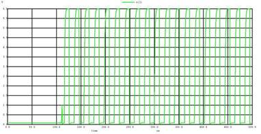
VIII. RESULTS
The results of simulation of the designed circuit is shown below. It displays the output of astable multivibrator with variable frequency and Duty cycle.
|
Resistors |
Capacitor |
Freq. |
Duty |
||||
|
Cycle |
|||||||
|
R1 |
R2 |
R3 |
R4 |
C1 |
C2 |
||
|
10 k |
10 k |
220 |
220 |
3.03 |
5.05 |
17.8 |
37.5% |
|
u |
u |
Hz |
|||||
|
10 k |
10 k |
220 |
220 |
5.05 |
5.05 |
14.2 |
50% |
|
u |
u |
Hz |
|||||
|
10 k |
10 k |
220 |
220 |
5.05 |
3.03 |
17.8 |
62.5% |
|
u |
u |
Hz |
|||||
|
1.4 |
1.4 |
100 |
100 |
10 p |
10 p |
50 |
50% |
|
meg |
meg |
k |
k |
KHz |
|||
Fig 1.2 Experimental Results
Output from NGSpice simulator for Different frequencies and
Duty cycle:
1. F = 17.8 Hz, Duty Cycle = 37.5%
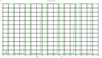
2. F = 14.2 Hz, Duty Cycle = 50%
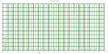
3. F = 17.8 Hz, Duty Cycle = 62.5%
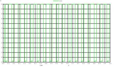
4. F = 50 KHz, Duty Cycle = 50%
X. A DVANTAGE s AND D ISADVANTAGE s
Advantages:
1. This circuit is less expensive than crystal clocks.
2. The circuit can has variable duty cycle from 10% to 50%
3. The output frequency of circuit can be varied from 2 Hz to 100 KHz.
Disadvantages:
If the characteristics of capacitors changes slightly then there is a probability that output waveform becomes too small to be used in the applications.
IX. A PPLICATIONS
1. This circuit can be used as clock input to sequential circuits.
2. It can be used in transmission and reception of radio waves.
3. For Morse code generators this circuit can be used.
XI. C ONCLUSION
In this project, the astable multivibrator is demonstrated through NGSpice software and these results from the both circuits resembles with the theoretical value.
The circuit purposed here is very simple, easily implementable and practical too as well as cost effective and hence can be used as an oscillator circuit over other conventional ones for simple analysis at educational level.