In Digital Designs, our primary aim is to create an Integrated Circuit (IC). A Circuit configuration or arrangement of the circuit elements in a special manner will result in a particular Logic Family. Electrical Characteristics of the IC will be identical. In other words, the different parameters like Noise Margin, Fan In, Fan Out etc will be identical.
Different ICs belonging to the same logic families will be compatible with each other.
The basic Classification of the Logic Families are as follows:
A) Bipolar Families
B) MOS Families
C) Hybrid Devices
A) Bipolar Families:
1. Diode Logic (DL)
2. Resistor Transistor Logic (RTL)
3. Diode Transistor Logic (DTL)
4. Transistor- Transistor Logic (TTL)
5. Emitter Coupled Logic (ECL) or Current Mode Logic (CML)
6. Integrated Injection Logic (IIL)
B) MOS Families:
1. P-MOS Family
2. N-MOS Family
3. Complementary-MOS Family
• Standard C-MOS
• Clocked C-MOS
• Bi-CMOS
• Pseudo N-MOS
• C-MOS Domino Logic
• Pass Transistor Logic
C) Hybrid Family:
Bi-CMOS Family
Diode Logic
In DL (diode logic), only Diode and Resistors are used for implementing a particular Logic. Remember that the Diode conducts only when it is Forward Biased.
Disadvantages of Diode Logic
• Diode Logic suffers from voltage degradation from one stage to the next.
• Diode Logic only permits OR and AND functions.
Resistor Transistor Logic
In RTL (resistor transistor logic), all the logic are implemented using resistors and transistors. One basic thing about the transistor (NPN), is that HIGH at input causes output to be LOW (i.e. like a inverter). In the case of PNP transistor, the LOW at input causes output to be HIGH.
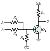
Advantage:
- Less number of Transistors
Disadvantage:
- High Power Dissipation
- Low Fan In
Diode Transistor Logic
In DTL (Diode transistor logic), all the logic is implemented using diodes and transistors.
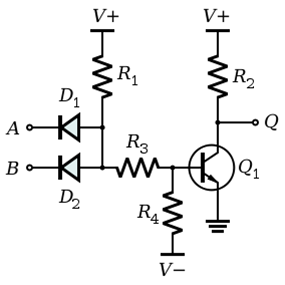
Disadvantage:
• Propagation Delay is Larger
Transistor Transistor Logic
In Transistor Transistor logic or just TTL, logic gates are built only around transistors.
TTL Logic has the following sub-families:
• Standard TTL.
• High Speed TTL
• Low Power TTL.
• Schhottky TTL.
• Low Power Schottky TTL
• Advanced Schottky TTL
• Advanced Low Power Schottky TTL
• Fast Schottky
Emitter Coupled Logic
The main specialty of ECL is that it is operating in Active Region than the Saturation Region. That is the reason for its high speed operation. As you can see in the figure, the Emitters of the Transistors Q1 and Q2 are coupled together.
Disadvantage:
• Large Silicon Area
• Large Power Consumption
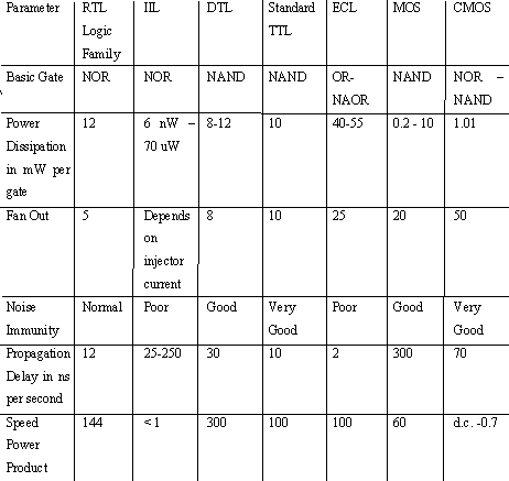
Some Characteristics we consider for the selection of a particular Logic Family are:
• Supply voltage range
• Speed of response
• Power dissipation
• Input and output logic levels
• Current sourcing and sinking capability
• Fan in
• Fan-out
• Noise margin
Introduction of Digital logic families
Miniature, low-cost electronics circuits whose components are fabricated on a single, continuous piece of semiconductor material to perform a high-level function. This IC is usually referred to as a monolithic IC first introduced in 1958. The digital ICs are categorized as,
1. Small scale integration SSI <12 no of gates
2. Medium scale integration MSI 12 to 99 no of gates
3. Large scale integration LSI 100 to 9999 no of gates
4. Very large scale integration VLSI 10,000 or more
In this section, we will be concern only with the digital IC. Digital IC can be further categorized into bipolar or unipolar IC.
Bipolar ICs are devices whose active components are current controlled while unipolar ICs are devices whose active components are voltage controlled.
IC Packaging
1. IC packaging Protect the chip from mechanical damage and chemical contamination.
2. Provides a completed unit large enough to handle.
3. So that it is large enough for electrical connections to be made.
4. Material is molded plastic, epoxy, resin, or silicone. Ceramic used if higher thermal dissipation capabilities required. Metal/glass used in special cases.
Three most common packages for ICs are
a) dual-in-line (DIPS) (most common)
b) flat pack
c) axial lead (TO5)

Characteristics of Digital ICs
Input /Output voltage level:
The following currents and voltages are specified which are very useful in the design of digital systems.
High-level input voltage, VIH : This is the minimum input voltage which is recognized by the gate as logic 1.
Low-level input voltage, VIL: This is the maximum input voltage which is recognized by the gate as logic 0.
High-level output voltage, VOH: This is the minimum voltage available at the output corresponding to logic 1.
Low-level output voltage, VOL: This is the maximum voltage available at the output corresponding to logic 0.
High-level input current, IIH : This is the minimum current which must be supplied by a driving source corresponding to 1 level voltage.
Low-level input current, IIL: This is the minimum current which must be supplied by a driving source corresponding to 0 level voltage.
High-level output current, IOH: This is the maximum current which the gate can sink in 1 level.
Low-level output current, IOL: This is the maximum current which the gate can sink in 0 level.
High-level supply current, ICC (1): This is the supply current when the output of the gate is at logic 1.
Low-level supply current, ICC (0): This is the supply current when the output of the gate is at logic (0).
Propagation Delay:
Definition: The time required for the output of a digital circuit to change states after a change at one or more of its inputs. The speed of a digital circuit is specified in terms of the propagation delay time. The delay times are measured between the 50 percent voltage levels of input and output waveforms. There are two delay times, tpHL: when the output goes from the HIGH state to the LOW state and tpLH, corresponding to the output making a transition from the LOW state to the HIGH state. The propagation delay time of the logic gate is taken as the average of these two delay times.
Fan-in
Defination: Fan-in (input load factor is the number of input signals that can be connected to a gate without causing it to operate outside its intended operating range. expressed in terms of standard inputs or units loads (ULs).
Fan-out
Defination:Fan-out (output load factor) is the maximum number of inputs that can be driven by a logic gate. A fanout of 10 means that 10 unit loads can be driven by the gate while still maintaining the output voltage within specifications for logic levels 0 and 1.
Digital IC gates are classified not only by their logic operation, but also by the specific logic circuit family to which it belongs. Each logic family has its own basic electronic circuit upon which more complex digital circuits and functions are developed.
Different types of logic gate families :
RTL : Resistor Transistor Logic gate family
DCTL : Direct Coupled Transistor Logic gate family
RCTL : Resistor Capacitor Transistor Logic gate family
DTL : Diode Transistor Logic gate family
TTL : Transistor Transistor logic gate family
IIL : Integraeted Injection gate family