Home > VHDL > Shift Registers > RAM
Random Access Memory
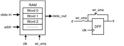
Here, the implementation of RAM (random access memory) is shown. The system has a data input bus (data_in), a data output bus (data_out), an address bus (addr), along with clock (clk) and write enable (wr_ena) pins. When wr_ena is given, at the next rising edge of clk the vector present at data_in stored in the position given by addr. The capacity chosen for the RAM is 16 words of length 8 bits each. Notice that the code is totally generic. Simulation results from the circuit synthesizad with the VHDL code are shown below.
LIBRARY ieee;
USE ieee.std_logic_1164.all;
ENTITY ram IS
GENERIC ( bits: INTEGER := 8; -- # of bits per word
words: INTEGER := 16); -- # of words in the memory
PORT ( wr_ena, clk: IN STD_LOGIC;
addr: IN INTEGER RANGE 0 TO words-1;
data_in: IN STD_LOGIC_VECTOR (bits-1 DOWNTO 0);
data_out: OUT STD_LOGIC_VECTOR (bits-1 DOWNTO 0));
END ram;
ARCHITECTURE ram OF ram IS
TYPE vector_array IS ARRAY (0 TO words-1) OF
STD_LOGIC_VECTOR (bits-1 DOWNTO 0);
SIGNAL memory: vector_array;
BEGIN
PROCESS (clk, wr_ena)
BEGIN
IF (wr_ena='1') THEN
IF (clk'EVENT AND clk='1') THEN
memory(addr) <= data_in;
END IF;
END IF;
END PROCESS;
data_out <= memory(addr);
END ram;