Home > CMOS Processing Technology > planar process technology
Planar Process Technology :
Technological evolutions toward integrated circuits began with development of diode and the invention of the transistor in late 1940s at that time semiconductor of interest was Germanium. After that silicon becomes a major workhorse for IC technology because of its ability to form a stable and controllable silicon dioxide layer. Two chemical properties of Si-SiO 2 system are of basic importance to silicon technology. First, selective etching is possible using liquid or gaseous etchants and second is silicon dioxide can be used to shield on underlying silicon crystal from dopant impurity atoms brought to the surface either by high energy ion beams or from a high temperature gaseous diffusion source. Using these features dopant atoms can be introduced into areas on the silicon that are not shielded by thick silicon dioxide.
The shielded regions can be accurately defined by using photosensitive polymer films exposed with photographic masks. The polymer pattern protects selected oxide regions on the silicon surface when it is immersed in hydrofluoric acid bath or exposed to gas phase etchants, this forms a surface consisting of base silicon windows in silicon dioxide layer. This selective etching process originally developed. For lithographic printing applications which forms a very small patterns. When the silicon sample is placed in chamber that deposits dopant atoms on the surface then the dopant atoms enter the silicon only at the exposed silicon windows.
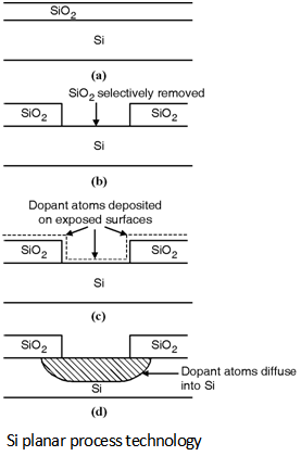
Proper sequencing and repetition of the oxidation, patterning and dopant addition operations, p and n dopant atoms are introduced into selective regions. This process is called as the silicon planar process which gives a major breakthrough to the IC fabrication technology. The basic silicon planar process is shown in Figure below. This process is called as the planar process because it is a process that produces device structures through a sequence of steps carried out near the surface plane of the silicon crystal.
The most important steps in the planar process are shown in Figure.The steps include :
a) Formation of masking oxide layer
b) Selective removal of SiO2
c) Deposition of dopant atoms on or near the wafer surface.
d) Diffusion of dopant atoms into exposed silicon regions.
The minimum feature size on an integrated circuit has continued to evolve at a rapid rate decreasing from 8 mm in 1969 to 90 nm today. Along with the rapid decrease in minimum feature size, the size of the IC chip continuously increasing. Because of the combination of smaller feature size the number of transistors on an IC chip increasing more rapidly doubling every 18-24 months. This rapid increase is made possible by continuing technological developments.
This chapter discusses the CMOS IC technology in details. CMOS integrated circuits are fabricated on thin circular slices of silicon called wafers. The first half of the chapter discusses about the CMOS IC fabrication technology and in the 2nd half we will discuss design rules and components on an integrated circuit.
