Home > CMOS Processing Technology > p well Process
p-well Process :
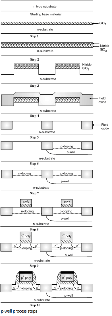
The fabrication steps of p well process are same as that of an n-well process except that instead of n-well a p-well is implanted . The process steps involved in p-well process are shown in Figure below. The process starts with the n type substrate.
Step 1 : A thin layer of SiO2 is deposited which will serve as the pad oxide.
Step 2 : A thicker sacrificial silicon nitride layer is deposited by chemical vapour deposition (CVD).
Step 3 : A plasma etching process is used to create trenches used for insulating the devices.
Step 4 : The trenches are filled with SiO2 which is called as the field oxide.
Step 5 : To provide flat surface chemical mechanical planerization is performed and also sacrificial nitride and pad oxide is removed.
Step 6 : The p-well mask is used to expose only the p-well areas, after this implant and annealing sequence is applied to adjust the well doping. This is followed by a second implant step to adjust the threshold voltage of the NMOS transistor.
Step 7 : Implant step is performed to adjust the threshold voltage of PMOS transistor.
Step 8 : A thin layer of gate oxide and polysilicon is chemically deposited and patterned with the help of polysilicon mask.
Step 9 : Ion implantation to dope the source and drain regions of the PMOS (p+) and NMOS (n+) transistors, this will also form n + polysilicon gate and p+ polysilicon gate for NMOS and PMOS transistors respectively. Hence this process is called as self aligned process.
Step 10 : Then the oxide and nitride spacers are formed by chemical vapour deposition.
Step 11 : In this step contact or via holes are etched, metal is deposited and patterned. After the deposition of last metal layer final passivation or overglass is deposited for protection.
