Home > CMOS Processing Technology > n well Process
n-well Process :
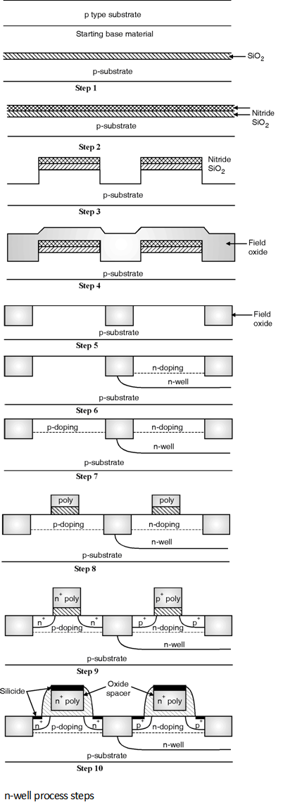
The process steps involved in the n-well process are shown in Figure below.
The process starts with a p-substrate.
Step 1 : A thin layer of SiO2 is deposited which will serve as a the pad oxide.
Step 2 : Deposition of a thicker sacrificial silicon nitride layer by chemical vapour deposition (CVD).
Step 3 : A plasma etching process using the complementary of the active area mask to create trenches used for insulating the devices.
Step 4 : The trenches are filled with SiO2 which is called as the field oxide.
Step 5 : To provide flat surface chemical mechanical planerization is performed and also sacrificial nitride is removed.
Step 6 : The n-well mask is used to expose only the n-well areas, after this implant and annealing sequence is applied to adjust the well doping. This is followed by second implant step to adjust the threshold voltage of the PMOS transistor.
Step 7 : Implant step is performed to adjust the threshold voltage of NMOS transistor.
Step 8 : A thin layer of gate oxide and polysilicon is chemically deposited and patterned with the help of polysilicon mask.
Step 9 : Ion implantation to dope the source and drain regions of the PMOS (p+) and NMOS (n+) transistors, this will also form n + polysilicon gate and p+ polysilicon gate for NMOS and PMOS transistors respectively. Hence this process is called as self aligned process.
Step 10 : Then the oxide or nitride spacers are formed by chemical vapour deposition.
Step 11 : In this step contact or via holes are etched, metal is deposited and patterned. After the deposition of last metal layer final passivation or overglass is deposited for protection.
