Home > CMOS Processing Technology > CMOS Process Enhancements
CMOS Process Enhancements :
In the Analog, Digital or RF CMOS integrated circuits along with transistors other elements such as interconnects, resistors, capacitors are to be integrated on chip. In order to achieve this, enhancements in CMOS process technology is required. The main goals of adding CMOS enhancements are :
(1) To provide on chip capacitors for analog circuits.
(2) To provide on chip resistors.
(3) To provide routing of interconnects.
The enhancements in CMOS technology are :
(1) Multilevel metal layers.
(2) Multilevel poly layers.
To enhance the CMOS technology the bipolar transistors can be integrated on chip in CMOS technology and this forms the BiCMOS technology. Here we will discuss the processing requirements to make these devices on chip.
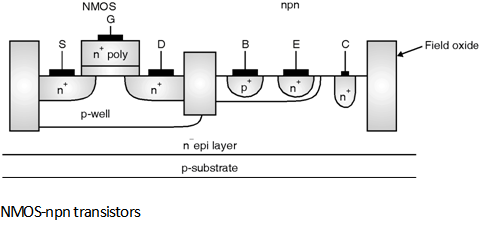
Figure below shows the cross-section of BiCMOS process in which NMOS and npn transistor are fabricated on the same substrate.

The starting material is p substrate on which n type epitaxial layer is grown. To form the NMOS transistor a p well is diffused in selected area. And n+ diffusions form the source and drain contacts. The nepilar is diffused with the p+ diffusion which forms the base for the npn transistor both the devices i.e. NMOS and npn transistors are isolated by field oxide.
Interconnect :
The most important enhancement in CMOS processes is the additions of signal and power supply routing layers. The advantage of this type of routing is it improves power and clock distribution to the different modules inside the chip. The interconnect layers involved in process are :
(1) Metal interconnect
(2) Polysilicon interconnect
(3) Local interconnect.
The second layer of metal interconnect (Metal 2) is required for digital Integrated circuits. The connection between first metal layer (Metal 1) and second metal layer (Metal 2) is established with the help of via. For high speed chips third metal layer (Metal 3) is also required.
Polysilicon Interconnect layers are used in ICs because of its high melting points as compare to Al. But the major problem with polysilicon interconnect is it has high sheet resistance because of this for long distance interconnects this provides significant delay.
If silicide is used as a interconnect layer for connecting different cells
then it is called as local interconnect. The important advantage of local
interconnect is it allows direct connection
between polysilicon and diffusion regions due to this metal contacts are
eliminated which reduces the chip area.
In order to create the on chip resistors n-well or polysilicon materials can be used. The resistance of a material is a function of the materials resistivity ‘r’ and the dimensions of the material. Figure below shows the slab of the material. The resistance between the two leads A and B is given as,
R = × = Rsheet
where Rsheet is the sheet resistance of material in W/square.

Figure below shows the layout of capacitors used in integrated circuits.
As shown in Figure the capacitor can be formed by adding extra poly silicon layer. In Figure (b) allows contacts to poly to be placed directly on top of the thin oxide which is the isolation between two poly plates. The bottom plate of the capacitor is made using poly 1 while the top plate where area determines the capacitance is made using poly 2. A circular disc is used for poly 2. In Figure (a) the contact to poly is lying over the field region. In this, sharp corners are avoided in the layout.
